鑫景福致力于滿足“快速服務,零缺陷,輔助研發(fā)”PCBA訂購單需求。


行業(yè)新聞

CharacteristICs and Applications of PCB Surface Treatment Technology
I. Introduction
With the continuous improvement of human's requirements for the living environment Lead and bromine are hot topics at present; Lead free and halogen-free will affect PCB in many aspects Although PCB boards are not very large in the surface treatment process at present, which seems to be a relatively remote matter, it should be noted that long-term slow changes will lead to huge changes With the growing demand for environmental protection, the surface treatment process of PCB board s will change greatly in the future
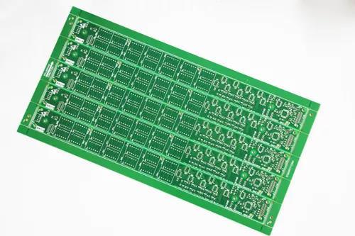
PCB board

2. Purpose of surface treatment
The basic purpose of surface treatment is to ensure good solderability or electrical properties. Because copper in nature often exists in the air in the form of oxides, it is unlikely to exist as raw copper for a long time and requires additional copper treatment Although the strong flux can be used to remove most copper oxides in subsequent assembly, the strong flux itself is not easy to eliminate. Therefore, the industry usually does not use strong flux
3. Five common surface treatment processes
There are many surface treatment processes for PCB Common ones are hot air leveling, organic coating, electroless nickel plating/immersion gold, immersion silver and immersion tin, which will be introduced one by one below
1) Hot air leveling
Hot air leveling, also known as hot air solder leveling, is a process PCB and flattening (blowing) it with heated compressed air to form a layer that resists copper oxidation and provides good reliability Weldable coatings In the hot air leveling process, copper tin intermetallic compound is formed at the joint between solder and copper The thickness of solder used to protect the copper surface is approximately 1-2 mils The PCB board hot air leveling is immersed in molten solder; Before the solder is solidified, the air knife blows the liquid solder; The air knife can make the solder form meniscus on the copper surface to prevent solder bridging Hot air leveling is divided into vertical and horizontal types It is generally believed that horizontal type is better, mainly because the leveling layer of horizontal hot air is more uniform and can realize automatic production The general process of hot air leveling is: micro etching preheating flux coating tin spraying cleaning
2) Organic coating
The organic coating process is different from other surface treatment processes, which acts as a barrier between copper and air; The SIMple process and low cost of organic coating make it widely used in the industry The molecules of the early organic coating are imidazole and benzotriazole, which play an anti rust role. The molecule is mainly benzimidazole, which is a PCB on copper with a chEMIcal bond nitrogen functional group In the subsequent welding process, if only one layer of organic coating on the copper surface is unacceptable, there must be many layers This is why liquid copper is usually added to the chemical tank After coating, the coating adsorbs copper; Then the organic coating molecules of the second layer are combined with copper until 20 or even hundreds of organic coating molecules are assembLED on the copper surface, which can ensure multiple reflow soldering. Tests show that the organic coating process can maintain good performance in a variety of lead-free soldering processes The general process of the organic coating process is: degreasing - micro etching - pickling - pure water cleaning - organic coating - cleaning. Compared with other surface treatment processes, the process control is easier
3) Electroless Nickel/Immersion Gold
The electroless nickel/gold plating process is not as simple as organic coating Electroless nickel plating/immersion gold seems to give PCB; In addition, the electroless nickel plating/gold DIPping process does not play the role of rust prevention as the organic coating does Layer, which can be used for long-term use of PCB boards and achieve good power efficiency Therefore, electroless nickel plating/gold dipping is to wrap a layer of thick nickel gold alloy with good power efficiency on the copper surface, which can protect PCB for a long time; In addition, it also has the environmental protection that other surface treatment processes do not have P Patience The reason for nickel plating is the mutual diffusion of gold and copper, and the nickel layer prevents the diffusion between gold and copper; Without the nickel layer, gold would diffuse into copper within hours Another advantage of electroless nickel plating/gold immersion is the strength of nickel, because only 5 microns of nickel can limit the Z-direction expansion at high temperatures In addition, electroless nickel/gold immersion can also prevent the dissolution of copper, which will be beneficial to lead-free assembly The general process of electroless nickel plating/gold leaching process is: pickling - micro etching - pre leaching - activation - electroless nickel plating - electroless gold leaching. There are mainly 6 chemical tanks, involving nearly 100 chemicals. It is difficult to control this process
4) Immersion silver
The immersion silver process is between organic coating and electroless nickel/immersion gold The process is relatively simple and fast; It is not as complex as electroless nickel plating/immersion gold, nor does it cover the ground with a thick armor PCB, but it still provides good power efficiency Silver is the younger brother of gold. It can maintain good solderability, humidity and pollution even under high temperature, but it will lose luster Immersed silver does not have the good physical strength of electroless nickel/immersion gold because there is no nickel under the silver layer In addition, silver immersion has good storage efficiency, and after several years of silver immersion, no major problems will occur in the assembly process Immersed silver is a displacement reaction, which is almost a layer of submicron pure silver coating SometiMES the silver immersion process also contains some organic substances, which mainly prevent silver corrosion and eliminate silver migration; It is usually difficult to measure this thin layer of organic matter. Analysis shows that the weight of organic matter is less than 1%
5) Immersion Tin
Since all current solders are based on tin, the tin layer can match any type of solder From this point of view, the tin dipping process has broad prOSPects for development However, tin whiskers appear after the last PCB tin dipping process, and the migration of tin whiskers and tin during welding will bring reliability problems. In conclusion, the tin dipping process is limited Later, adding organic additives to the tin impregnation solution can make the tin layer structure have a granular structure, which overcomes the previous problems, and has good thermal stability and solderability The tin dipping process can form a flat copper tin intermetallic compound, which makes the immersion tin have the same good solderability as the hot air leveling without worrying about the hot air leveling; Immersed tin also has no diffusion problem between electroless nickel plating/immersion gold metals - copper tin intermetallics can be firmly bonded together The tin dipping plate shall not be stored for too long, and the assembly must be carried out according to the tin dipping sequence
6) Other surface treatment processes
There are few applications of other surface treatment processes. Let's take a look at relatively many nickel gold electroplating and electroless palladium plating processes Nickel gold electroplating is the originator of surface treatment process for PCB boards Since PCB board s, it has gradually evolved into other methods First, paint a layer of nickel PCB on the wire surface, and then paint a layer of gold Nickel plating is mainly used to prevent diffusion between gold and copper Now there are two types of electrified nickel gold: soft gold plating (pure gold, the gold surface does not look bright) and hard gold plating (the surface is smooth and hard, wear-resistant, containing cobalt and other elements, and the gold surface looks bright) Soft gold is mainly used for gold wire in chip packaging; Hard metal is mainly used for power interconnection in non welding places Considering the cost, the industry usually uses image transmission to reduce the use of gold through selective electroplating At present, the use of selective gold plating in the industry continues to increase, mainly due to the difficulty in controlling the chemical nickel plating/gold leaching process Under normal circumstances, welding will cause the electroplated gold to become brittle, which will shorten its service life; However, electroless nickel plating/immersion gold is very thin and uniform, with little embrittlement The electroless palladium plating process is similar to the electroless nickel plating process the main process is to reduce palladium ions to palladium on The catalytic surface by a reducing agent (such as sodium dihydrogen hydrate) The advantages of electroless palladium plating are good welding reliability, thermal stability and surface flatness
4. The choice of surface treatment technology
The choice of surface treatment process mainly depends on the type of final assembly components; The surface treatment process will affect the production, assembly and final use of PCB The following details the use of five common surface treatment processes
1) Hot air leveling
Hot air leveling once dominated the PCB surface treatment process In the 1980s, more than three quarters of PCB boards used hot air leveling process, but in the past deCADe, the industry has been reducing the use of hot air leveling process It is estimated that there are about 25% - 40% PCB boards at present Use hot air leveling process Dirty, SMElly and dangerous hot air leveling process has never been the most popular process, but it is an excellent process for larger parts and wires with larger spacing With higher PCB density, the flatness of hot air leveling will affect subsequent assembly; Therefore, HDI boards usually do not use the hot air leveling process With the progress of science and technology, the industry has developed hot air leveling process P suitable for QF and BGA with SMAll assembly spacing, but there are few practical applications At present, some factories use organic coating and electroless nickel plating/gold dipping process to replace the hot air leveling process; The development of science and technology has also led some factories to adopt tin dipping and silver dipping processes In addition, the lead-free trend in recent years further restricts the use of hot air leveling Although the so-called lead-free hot air leveling has occurred, it may involve equipment compatibility problems


抖音二維碼

Q Q二維碼

微信二維碼
點擊
然后
聯(lián)系
然后
聯(lián)系
電話熱線
13410863085Q Q

微信

- 郵箱