鑫景福致力于滿足“快速服務(wù),零缺陷,輔助研發(fā)”PCBA訂購單需求。


行業(yè)新聞
PCB flip chip assembly technology
With the emergence of miniaturization and high-density packaging, the requirement of high-speed PCB high-precision assembly becoMES more critICal, and related assembly equipment and processes become more advanced and flexible Because flip chip has SMAller shape factor, smaller ball diameter and ball pitch than BGA or CSP, it provides unprecedented possibility for ball placement, substrate technology, data compatibility, manufacturing technology, and inspection equipment and methods Challenge Nowadays, Electronic devices have more and more miniaturization and high-density packaging forms, such as multi module packaging (MCM), packaging system (SiP), flip chip (FC, Flip Chip) and other applications The appearance of these technologies further blurs the boundary between packaging and secondary assembly Undoubtedly, with the emergence of miniaturization and high-density packaging, the requirements for high-speed and high-precision assembly become more critical, and related assembly equipment and processes become more advanced and flexible Because flip chip has smaller shape factor, smaller ball diameter and ball pitch than BGA or CSP, it provides unprecedented possibility for ball placement, substrate technology, data compatibility, manufacturing technology, and inspection equipment and methods Challenge These requirements are analyzed in detail below:
1. Installation pressure control requirements. Considering that the flip chip substrate of PCB is relatively fragile silicon, it is easy to break if a large pressure is applied during data recovery and flux impregnation. At the same time, small solder joints are easy to deform during this process. Therefore, relatively low installation pressure should be used as far as possible The general requirement is about 15.0g For ultra-thin wafers, such as 0.3 mm, it is sometimes necessary to control the installation pressure at 35g
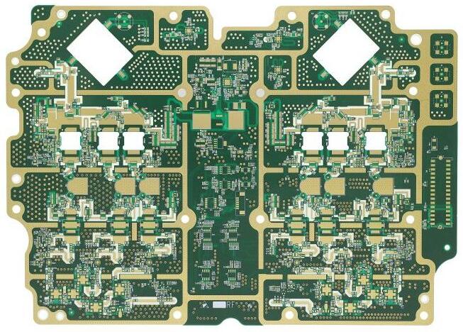
PCB board

2. The requirements for placement accuracy and stability are for equipment with ball distance less than 0 1 mm, what kind of placement precision is required to achieve high output? The warping and deformation of the substrate, the size and position deviation of the mask window, and the accuracy of the machine will affect the final placement accuracy We will not discuss the influence of substrate design and manufacturing on placement, but here we only discuss the placement accuracy of the machine
3. To answer the above questions, let's build a SIMple hybrid model:
1) Assume that the solver bumps of the flip chip PCB is spherical, and the corresponding pads on the subset are circular and have the same diameter;
2) It is assumed that there is no influence of substrate warpage and manufacturing defects;
3) Does not consider the effects of Theta and shock;
4) During the reflow soldering process, the device is self neutral. During the welding process, 50% of the contact between the solder ball and the wetted surface can be "pulLED up" Then, based on the above assumption, the left and right position evolution (X axis) or the front and rear position evolution (Y axis) is 50% of the pad size if the diameter of the 25 mm welding ball is 50 mm The ball is always on the mat For flip chip PCB board s, the diameter of solder ball is 25mm. If the process capacity Cpk reaches 1.33, the precision of the machine must reach 12mm
4. According to the requirements of CAMera and image processing technology, a digital camera with millions of graphic elements is required to process the s Digital cameras with higher points have higher magnification. However, the smaller the field of view (FOV), which means that large devices may need to "take pictures" many times The light source of the camera is usually a light-EMItting diode, which is divided into side light source, front light source and axial light source, and can be controlled independently Flip chip imaging light source PCB board uses side lights, headlights, or a combination of both So, how do you choose a monitor for a given device? This mainly depends on the image calculation For example, N points are required to distinguish a solder ball, and 2N points are required to distinguish the ball spacing Taking the Magellan digital camera on the universal instrument mounter as an example, it takes 4 points to distinguish a solder ball Select the camera and assume that all images are 7.5% of the actual object size The image processing PCB of flip chip reference point is similar to the common reference point In addition to global reference points, s usually uses local reference points for flip chip mounting PCB At this time, the cameras will be small (0.15-1.0mm). Refer to the above method for camera selection The choice of light source needs to be considered Generally, the light source of the monitor on the SMD head is red. When processing the reference point on the Flexible circuit board, the effect is poor, or even the reference point cannot be found The reason is that the surface of the reference point (coupler) The color is very close to the abstract color If the blue light source technology of general instruments is used, this problem can be solved well
5. Selection of nozzles
Since the flip chip abstract for PCB is silicon, the upper surface is very flat and smooth, the head is made of hard plastic materials, and it is equipped with a porous electrostatic discharge nozzle If you choose a nozzle with a rubber head, as the rubber ages, the equipment may adhere to the equipment during placement, causing the placement position to move or take away the equipment
6. Requirements for flux application device Flux application unit is an important part of controlling flux impregnation process The basic principle of its work is to obtain a stable flux film with a set thickness. In this way, each solder ball of the equipment can be easily immersed Use the same amount of flux The flux application unit must meet the following requirements:
1) It can meet the requirements of DIPping multiple devices with flux at the same time (such as dipping 4 or 7 pieces at the same time) to increase the output;
2) The unit for flux should be simple, easy to control and easy to clean;
3) It can handle a wide range of fluxes or solder pastes. The viscosity range of flux suitable for impregnation process is very wide, which can handle thinner and more viscous flux, and the obtained film thickness should be uniform;
4) The dipping process can be controlled. Due to different data, the dipping process parameters will also be different. In summary, the dipping process parameters must be controlled separately, such as downward acceleration, pressure, dwell time, upward acceleration, etc
7. Feeding technology is also critical to meet the requirements of feeder for high-speed and high-yield batch production Flip chip packaging method PCB board s mainly include: 2 * 2 or 4 * 4 inch JEDEC trees, 200mm or 300mm wafer trees (Wafer), and reed trees (Reel) The corresponding feeders are: fixed tray feeder, automatic stacking feeder, wafer feeder, and belt feeder All these feeding technologies must be able to feed at high speed. In addition, the wafer feeder also needs to be able to handle various equipment packaging methods, such as: equipment packaging can be JEDEC tray, or bare chips, or even complete chips in the machine Flip action Let's take an example to illustrate the characteristics of Unovis's bare die feeder (DDF Direct Die Feeder):
1) Can be used in hybrid circuits or sensors, system in package, RFID and 3D assembly;
2) The disc can be fed vertically to save space, and one machine can install multiple DDFs;
3) The chip can be flipped in DDF;
4) Can be installed on a variety of patch platforms.
8. Requirements for board support and positioning system. Some flip chip PCBs are used for flexible circuit boards or thin circuit boards At this time, the plane support of the base plate is very important


抖音二維碼

Q Q二維碼

微信二維碼
點(diǎn)擊
然后
聯(lián)系
然后
聯(lián)系
電話熱線
13410863085Q Q

微信

- 郵箱