鑫景福致力于滿足“快速服務(wù),零缺陷,輔助研發(fā)”PCBA訂購單需求。


行業(yè)新聞
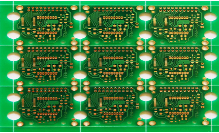
BGA for SMT chip processing is a packaging method. BGA is the abbreviation of BallGridArray in English, whICh is translated into ball grid array packaging in Chinese. In the 1990s, along with the continuous development of electronic technology, the IC processing speed was also continuously improved. The number of I/O pins on the integrated circuit chip continued to increase. Elements at all levels clearly put forward higher requirements for IC packaging. In addition, in order to consider the development of electronic equipment towards micromation and precision, BGA packaging CAMe out and was invested in production. The following technical professional SMT chip processing factory, Pete High Precision, briefly introduces the basic processing information of BGA to everyone.
1、 Steel MESh
In specific processing, the thickness of the steel mesh is generally, but in the welding processing of BGA devices, the thick steel mesh is likely to lead to tin bonding. According to Pater's high-precision surface assembly production experience, the steel mesh with thickness is very suitable for BGA devices, and can also moderately expand the total area of the steel mesh opening.
2、 Solder paste
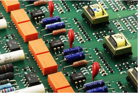
The foot spacing of BGA device is SMAll, so the solder paste used also stipulates that the particles of metal materials should be small, and excessive particles of metal materials will cause tin bonding in SMT processing.
3、 Welding temperature setting
Reflow soldering furnace is generally used in the whole process of SMT chip processing. Before welding BGA packaged components, the temperature of each area must be set according to the processing regulations and the temperature around the spot welding must be detected with a thermal resistance camera.
4、 Inspection after welding
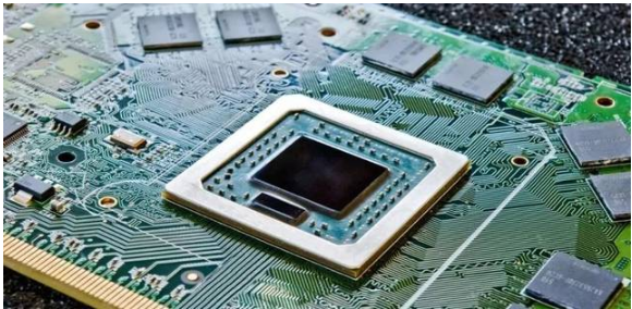
After SMT processing, BGA packaged devices should be rigorously tested to prevent some chip defects.
SMT chip processing
5、 Advantages of BGA packaging:
1. Improve the rate of finished products;
2. Electric heating performance improvement;
3. Reduced volume and mass;
4. Parasitic parameters decrease;
5. Small signal transmission delay;
6. Increase the frequency of use;
7. High credibility of goods;
6、 Defects of BGA package:
1. The inspection after welding must be carried out according to X-ray;
2. The cost of electronic production increases;
3. Cost increase;
Because of the packaging characteristics of BGA, it is very difficult to weld the SMT chip, and it is also difficult to operate the casting defects and repair, so as to ensure the welding quality of BGA devices. SMT chip processing plants generally pay attention to the customization of processing regulations from the following aspects.
Our company's PCB high-quality SMT chip processing, SMT OEM production substitute service project, one-stop PCBA processing, electronic processing, and PCB technology professional electronic processing factory.


抖音二維碼

Q Q二維碼

微信二維碼
點擊
然后
聯(lián)系
然后
聯(lián)系
電話熱線
13410863085Q Q

微信

- 郵箱