鑫景福致力于滿足“快速服務,零缺陷,輔助研發”PCBA訂購單需求。


行業新聞
Pcb multilayer board is a kind of unique printed board, and its memory "address" is generally unique, for example, there will be memory in the circuit board. This kind of Multilayer board can help the equipment to connect and disconnect various different routes. It is worth mentioning that it can also have the practICal effect of insulating layer, and it is not easy to make electricity collide with electricity, which is sure of safety.
If you want to apply it to a PCB multilayer board with good characteristics, you must carefully plan it, and then tell us how to design the PCB multilayer board.
PCB Multilayer Board Design Scheme
1. Definition of pcb multilayer board appearance design, specification and overlapping layers
1) All printed boards have the problem of matching assembly lines with other parts. Therefore, the appearance design and specifications of printed boards must be based on the entire equipment structure of the commodity. However, from the perspective of production process flow, it should be as SIMple as possible. Generally, it is a square with a narrow width to height ratio, which is conducive to improving the productivity of the assembly line and reducing labor costs.
2) The number of overlapping layers must be determined according to the provisions of power circuit characteristics, board specifications and the aggregation level of the route. For double-layer printed boards, the use of four layer boards and Six layer boards is more common. According to the characteristics of four layer boards, there are two wire layers (component surface and welding surface), one power layer and one geological structure.
3) Each layer of multilayer board shall maintain symmetry, and it is better to have double copper layers, namely four, six, eight layers, etc. Due to different laminations, the surface is very easy to cause expansion and contraction, especially for multilayer boards with surface patches.
2. Position and placement of pcb multilayer board components
1) The location and placement of components should be considered first from the circuit principle level, and follow the direction of power circuit. Whether the placement is effective or not will immediately endanger the characteristics of the printed circuit board, especially the high frequency digital integrated circuit. The location and placement of components seem more stringent.
2) Effective placement of components, to some extent, has already foreshadowed the success of the PCB design. Therefore, under the condition of manually editing the printed circuit board and making decisions on the overall rational layout, a detaiLED analysis of the circuit principle should be carried out. First, the location of unique components (such as large-scale IC, high-power tubes, video signals, etc.) should be defined, and then other components should be allocated to minimize the factors that will cause impact.
3) On the other hand, it is necessary to consider the overall structure of the printed circuit board to prevent the components from being sorted unevenly. This not only harms the beauty of the printed circuit board, but also brings a lot of trouble to the assembly line and maintenance work.
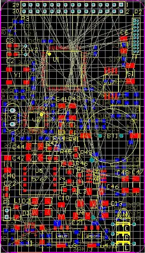
PCB multilayer board
3. Regulations on PCB wire layout and wiring area
In general, double-layer PCB wiring is carried out according to the role of power circuit. When wiring on the surface layer, it is stipulated that more wiring is carried out on the welding surface and less wiring is carried out on the component surface, which is beneficial to the maintenance and troubleshooting of PCB. Thin and dense wires and the affected power lines are generally distributed in the inner layer.
Large scale copper berths should be evenly distributed inside and on the surface, which will help reduce the expansion and contraction of the plate, and also enable a more symmetrical coating on the surface during the electroplating process. In order to avoid the damage of the printed wire caused by the appearance design, production and processing, and the short circuit fault of the virtual beam caused by the machining and manufacturing, the distance between the conductivity pattern in the wiring area of the inner surface layer and the plate edge should be more than 50mil.
4. Provisions on traverse direction and graphic boundary
The power supply layer, geological structure layer and data signal layer shall be separated for multi-layer PCB wiring to reduce the influence of switching power supply, ground and data signal. WirefraMES adjacent to double-layer printed boards shall be vertical to each other as much as possible, or shall follow the slash and curve diagram, instead of straight lines, to reduce the virtual beam coupling and influence of the base steel plate.
And the wire should be short wire as much as possible. Especially for SMAll data signal power circuit, the fewer wires, the smaller the resistor, and the smaller the impact. The power cord on the same layer shall be prevented from turning at an obtuse angle when changing direction. The width of the conductor shall be determined according to the provisions of the power circuit on the current and characteristic impedance. The input line of the switching power supply shall be larger and the relativity of the power line shall be smaller.
For general large digital boards, the graphic limit of switching power supply input line can be 50~80mil, and the graphic limit of power line can be 6~10mil.
Overall width of conductor: 0.5, 1, 0, 1.5, 2.0;
Allowable current: 0.8, 2.0, 2.5, 1.9;
Conductor resistor: 0.7, 0.41, 0.31, 0.25;
During wiring, the total width of the wire frame shall be as consistent as possible to prevent the wire from suddenly becoming wider and narrower, which is beneficial to the matching of characteristic impedance.
5. Stipulation of punching size and welding layer
1) The hole size of the components on the multilayer board is related to the pin size of the components used. If the hole size is too small, it will endanger the assembly and tin of the components; The drilling is too large, and the spot welding is not round enough during electric welding. Generally speaking, the calculation method of component hole diameter and welding layer size is:
2) Diameter of component hole=component pin diameter (or straight line)+(10-30mil)
3) Welding layer diameter ≥ component hole diameter+18mil
4) For the via diameter, the key is to determine the thickness of the finished board. For multilayer boards with high density, it should be controlled within the range of plate thickness: diameter ≤ 5:1. The calculation method of through hole welding layer is:
5) Diameter of via welding layer (VIAPAD) ≥ via diameter+12mil.
6. Provisions on power supply layer, geological structure system zoning and trepanning
For double-layer printed circuit board, there is at least one power supply layer and one geological structure. Because all the working voltages on the printed board are connected to the same power layer, it is necessary to carry out system partition protection on the power layer. The size of the system partition line is generally 20~80 mils. The working voltage is extremely high, and the system partition line is thicker.
At the junction of the welding hole, the power layer and the geological structure, in order to enhance its credibility and reduce the virtual connection caused by the heat absorption reaction of large-scale metal materials in the whole process of electric welding, the general connection plate should be designed with a pattern of flower holes. The diameter of the protective welding layer ≥ the drilling diameter+50 mil.
7. Provisions on safety interval
The setting of safety interval shall take into account the regulations on electricity safety. Generally speaking, the minimum interval of surface layer conductor shall not be less than 2mil, and the minimum interval of inner layer conductor shall not be less than 2mil. Under the condition that the wiring can be discharged, the interval should be the maximum value as far as possible, so as to improve the output rate of plate making process and reduce the potential safety hazards of common faults of finished boards.
8. Provisions for improving the anti-interference performance of the whole PCB
For the PCB design scheme of double-layer PCB, it is also important to pay attention to the anti-interference of the entire PCB. The general methods are:
a. Add filter capacitors around the switching power supply and ground of each IC, and the volume is generally 473 or 104.
b. For the relatively sensitive data signals on the printed circuit board, the accompanying shielded cables shall be added separately, and the wiring around the video signal shall be avoided as far as possible.
c. Select a valid destination address.


抖音二維碼

Q Q二維碼

微信二維碼
點擊
然后
聯系
然后
聯系
電話熱線
13410863085Q Q

微信

- 郵箱