鑫景福致力于滿足“快速服務(wù),零缺陷,輔助研發(fā)”PCBA訂購(gòu)單需求。


行業(yè)新聞
When hardware engineers contact PCB layout tools, PADS, Allegro, Protel and other tools from the beginning, they will inevitably contact the packaging and manufacturing of components. Whether it is chip mounted components, QFP, QFN, BGA, PGA, SOT23, TO263, MOIC and other chips, or passive components such as 040206030805, they must contact the package. Some are taken from the standard library, and some are made by ourselves. If you have seen many others', you will find that the same components have many subtle differences. These differences also more or less affect the quality of the patch and the effect of visual inspection, and more directly affect the service life of electronic products.
Today's topic is "component packaging". The production process of standard packaging is not described too much here. This is just to discuss the problems that often occur, and it will be beneficial to engineers, so as to improve the quality of SMT patches.
Layout design
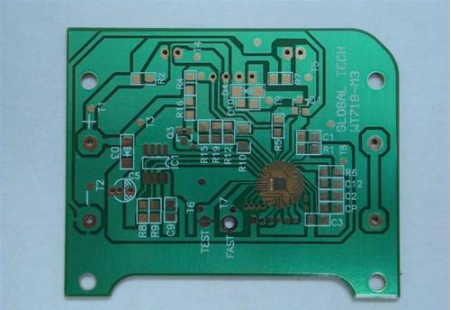
1. Silk screen. Silk screen may seem unimportant, without actual electrical characteristics, but it contains a lot of information. For two or three pin devices of different sizes, screen printing can ensure that the placement of the patch is correct. For diodes, tantalum capacitors, ESD and other polar devices, it is the only reference for visual inspection. For chip components, the position of a pin can be confirmed by screen printing. For BGA or QFN components, screen printing can visually detect whether the placement is correct. It is very helpful to judge the system failure. In addition, silk screen can also reflect many valuable information, such as company, board number, hardware settings, voltage, version and other information. Therefore, complete screen printing information has a great impact on the quality of the chip.
2. PCB pads, the size of which has always been a knotty problem for engineers. If the pads are made too large, it will increase the difficulty of wiring. If it is too SMAll, it will lead to poor contact. Generally, there will be layout guidance for complex chips. This is the first choice for layout reference. Generally speaking, for BGA or other chips, the pad size is 80% of the ball diameter.
3. Thermal pad. For power devices, thermal dissipation is becoming more and more important, whether it is a high range small mobile product or a large communication device. Heat dissipation during power is always the design center in hardware design. From the perspective of layout, the top and bottom layers below the power devices usually have a heat dissipation pad respectively, and some vias are regularly arranged at the top to connect them. The cooling path is chip ->chip package ->top layer cooling pad ->via ->bottom layer cooling pad ->air.
4. Connector. For PCB components that often need to be plugged and unplugged, such as earphone interface, board side buttons, HDMI interface, etc. Frequently, components fall off after several tiMES of plugging and unplugging, which will directly affect the user's experience. This is because the positioning pad is too small, or the positioning pad falls off, causing the component to fall off. We suggest that engineers manually increase the positioning pad and directly modify the solver mask layer and paste mask layer. If necessary, through holes can be directly added on the pad to increase the force on the pad.
5. Solder Mask and Paste Mask layers often interact with each other for component packaging. The Solder mask controls the green window opening of the PCB, while the Paste Mask is mainly responsible for the window opening of the steel mesh. Manual modification of these two layers is often encountered in some complex PCB designs. Often good use will get twice the result with half the effort.


抖音二維碼

Q Q二維碼

微信二維碼
點(diǎn)擊
然后
聯(lián)系
然后
聯(lián)系
電話熱線
13410863085Q Q

微信

- 郵箱