鑫景福致力于滿足“快速服務(wù),零缺陷,輔助研發(fā)”PCBA訂購單需求。


行業(yè)新聞
In PCB design, the design rule is the key to the success of a PCB design. All PCB designers' intentions and functions are driven and realized through the soul of PCB design rules. DelICate and detaiLED rule definition can help designers to be handy in PCB layout and routing, save engineers a lot of energy and time, help PCB designers to achieve excellent PCB design, and greatly facilitate PCB design.
The entire PCB design needs to follow the rule definition. Including the most basic electrical rules (spacing, short circuit and open circuit), wiring rules (line width, routing style, through hole style, fan out, etc.), and plane rules (connection mode of power ground plane layer, copper laying connection mode); And other commonly used auxiliary rules such as layout rules, manufacturing rules, rules, signal integrity rules, etc. After the PCB design is completed, you can also conduct a rule check Design Rule Check to re-examine your PCB design to see if there are any violations of the rules and make improvements
PCB design
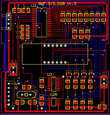
Rules and skills on PCB copper laying design. This paper introduces how to change the connection mode of copper paving and vias, and how to shrink the board edge during the copper paving design in Altium Designer.
How to make the via connection after copper coating not cross like the thermal pad
To make the via connection in the copper paved PCB not cross but directly connect, you can set the Plane - Polygon connect style in the Design Rule. The above default setting is the Relief connection connection mode, which is like a cross pattern connection like a hot pad. Yes, a rule is added and the object is set as IsVia of all vias in the Query statement. The rule is set to direct connection. After repainting copper. The cross pattern connection is canceled.
Set different spacing for copper laying (plate edge inside)
In PCB design and PCB manufacturing industry, in general, due to the mechanical consideration of the finished circuit board, or to avoid curling or electrical short circuit caused by the exposure of the copper sheet on the board edge, PCB engineers often shrink the large area of copper blocks relative to the board edge by 20 mils, instead of always laying the copper sheet to the board edge. There are many ways to deal with the copper skin shrinkage. For example, draw a keepout layer on the board edge, and then set the distance between copper paving and keepout. A SIMple method is introduced here, which is to set different safety distances for the copper laying objects. For example, the safety distance of the whole board is set to 10mil, while the copper laying object is set to 20mil. The plate edge can be shrunk by 20mil. At the same time, the possible dead copper in the device is removed. One action is worth more. There are many methods to process the edge shrinkage, and it is more clear and convenient to use the Query statement to precisely set the copper objects.
Let's discuss EMC interference in PCB design
11-10,2022


抖音二維碼

Q Q二維碼

微信二維碼
點擊
然后
聯(lián)系
然后
聯(lián)系
電話熱線
13410863085Q Q

微信

- 郵箱