鑫景福致力于滿足“快速服務(wù),零缺陷,輔助研發(fā)”P(pán)CBA訂購(gòu)單需求。


行業(yè)新聞
EMI Standard of circuit board -- How to Produce High Quality PCB
The electronIC signal of electronic equipment and the frequency of processor are constantly increasing, and the electronic system has become a complex equipment containing a variety of components and many subsystems. High density and high speed will aggravate the radiation of the system, while low voltage and high sensitivity will reduce the immunity of the system. Therefore, electromagnetic interference (EMI) really threatens the safety, reliability and stability of electronic equipment. When we design electronic products, PCB design is crucial to solving EMI problems. This article mainly explains what should be paid attention to in PCB design, so as to reduce the electromagnetic interference in PCB.
Definition of electromagnetic interference (EMI)
Electromagnetic interference (EMI) can be divided into radiation and conduction interference. Radiated interference means that the interference source interferes its signal to another electrical network with space as the medium. Conducted interference refers to the interference of signals on one electrical network to another electrical network by using conductive medium as the medium. In high-speed system design, integrated circuit pins, high-frequency signal lines and various plugs are common radiated interference sources in PCB design. The electromagnetic wave they emit is electromagnetic interference (EMI), which will affect the normal operation of themselves and other systems.
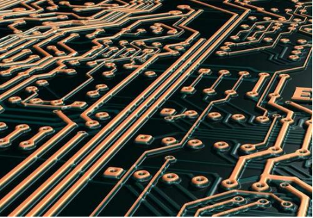
PCB Design Skills for Electromagnetic Interference (EMI)
Nowadays, there are many solutions to EMI problems in PCB design techniques, such as EMI suppression coating, appropriate EMI suppression parts, and EMI SIMulation design. The above videos describe ways to reduce EMI. Now let's briefly explain these techniques.
Tip 1: Common mode EMI interference source (such as the voltage drop formed by the transient voltage formed on the power bus at both ends of the inductance in the decoupling path)
- If low value inductors are used in the power supply layer, the transient signal synthesized by the inductors will be reduced, and the common mode EMI will be reduced.
- Reduce the length of the wiring from the power supply layer to the IC power supply pin.
- Use 3-6 mil PCB layer spacing and FR4 dielectric material.
Tip 2: Electromagnetic shielding
- Try to place the signal wiring on the same PCB layer and close to the power layer or ground plane.
- The power layer shall be as close to the ground plane as possible
Tip 3: Layout of parts (different layouts will affect the interference and anti-interference ability of the circuit)
- Block processing shall be carried out according to different functions in the circuit (such as demodulation circuit, high-frequency amplification circuit and frequency mixing circuit). In this process, strong and weak electrical signals shall be separated, and digital and analog signal circuits shall be separated
- The filter network of each part of the circuit must be connected nearby, which can not only reduce the radiation, but also improve the anti-interference ability of the circuit and reduce the chance of being interfered.
- The easily interfered parts shall be arranged to avoid interference sources as much as possible, such as the interference of CPU on the data processing board.
Tip 4: Consideration of wiring (unreasonable wiring will cause cross interference between signal lines)
- No wiring shall be close to the frame of PCB board to avoid wire breakage during fabrication.
- If the power line is wide, the loop resistance will be reduced.
- The signal line shall be as short as possible and the number of vias shall be reduced.
- The wiring at corners cannot be conducted by right angle method, and 135 ° angle is preferred.
- Digital circuit and analog circuit shall be isolated by ground wire, digital ground wire and analog ground wire shall be separated, and finally connected to power ground
Reducing electromagnetic interference is an important part of PCB design. As long as you think more about this side during design, it will be easier to pass product tests such as EMC tests.
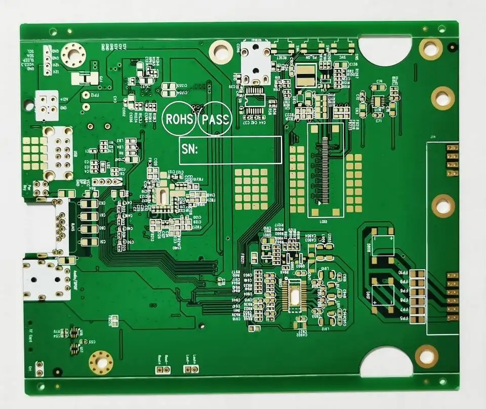
PCB manufacturers, PCB designers and PCBA manufacturers will explain the standards of circuit board EMI - how to produce high-quality PCBs


抖音二維碼

Q Q二維碼

微信二維碼
點(diǎn)擊
然后
聯(lián)系
然后
聯(lián)系
電話熱線
13410863085Q Q

微信

- 郵箱