鑫景福致力于滿足“快速服務,零缺陷,輔助研發”PCBA訂購單需求。


行業新聞
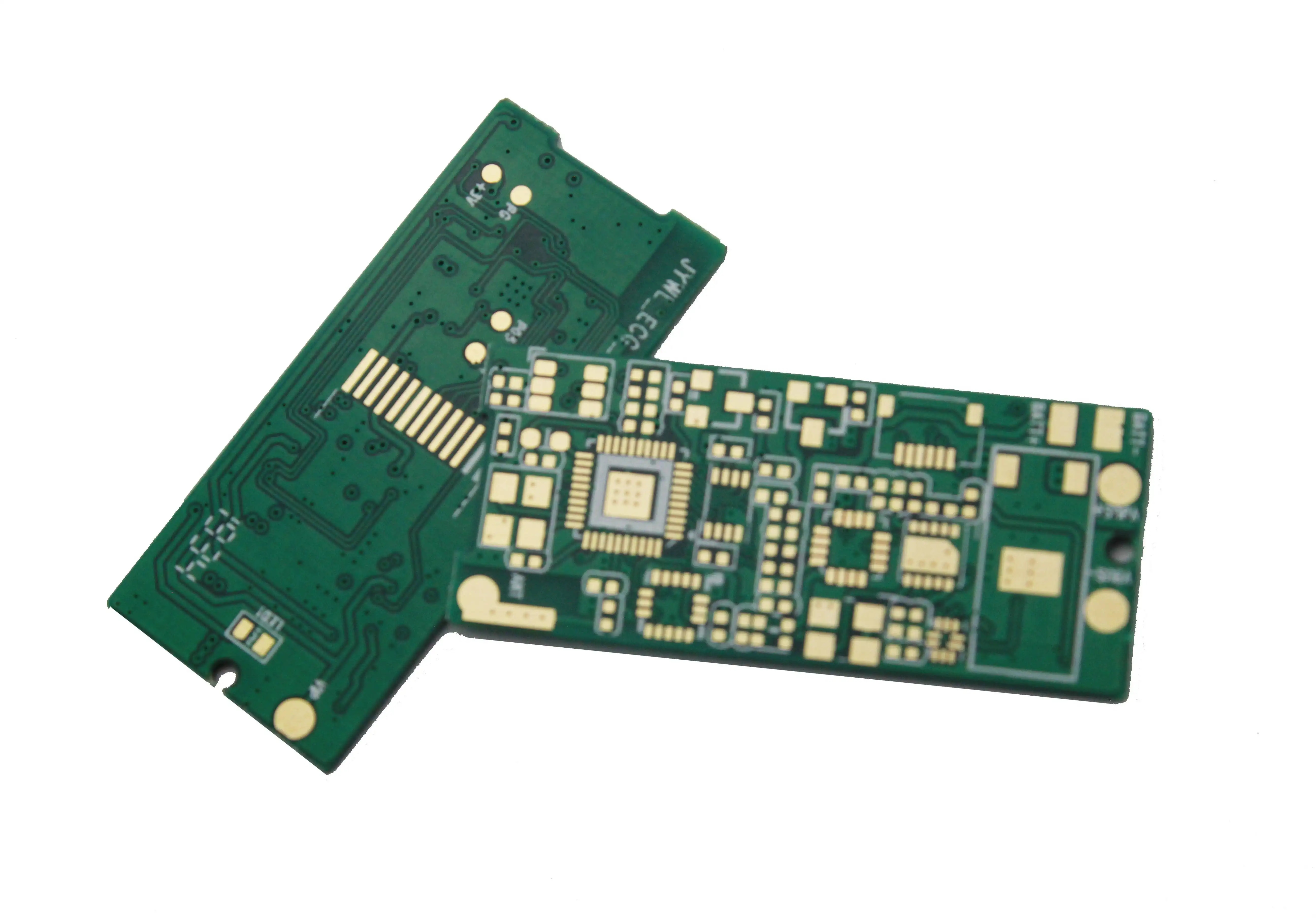
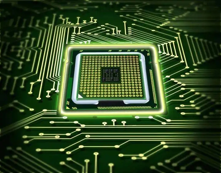
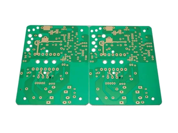
ElectronIC engineer editor explains PCB copper coating knowLEDge
For Xiaobai in PCB design, PCB copper coating is a very difficult skill. Today, the engineer Xiaobian will share with you what skills and methods PCB copper coating has. The copper coating of PCB is to take the idle space on the circuit board as the reference plane, and then fill it with solid copper, so filling solid copper is copper filling. The functions of copper coating include
: Reduce ground wire impedance, improve anti-interference ability and power efficiency; Connect with the ground wire to reduce the loop area.
The techniques for designing PCB copper coating include:
1. If there are many grounding parts of PCB, such as SGND, GND, AGND, etc., the most important "ground" shall be used as the standard reference for independent copper coating according to the different positions and wiring of PCB board, and the most basic is to separate the digital ground and analog ground for copper coating. Before copper-clad, the first thing to do is to thicken the corresponding power lines to form multiple deformation structures with different shapes to improve the performance of copper-clad.
2. Copper coating near the crystal oscillator. The crystal oscillator in the circuit is a high-frequency EMIssion source. Generally, copper coating is applied around the crystal oscillator, and then the shell of the crystal oscillator is separately grounded.
3. Single point connection of different "ground" is generally through 0 ohm resistance/magnetic bead/inductance connection;
4. If the island (dead zone) problem is large, SIMply add and define a "ground" via.
5. At the beginning of wiring, the ground wire should be treated equally. When wiring, the ground wire should be well laid. It is not possible to eliminate the connected ground pin by adding vias after copper coating. Such effect is very bad.
6. It is better not to have sharp corners (=180 degrees) on the board, because from the electromagnetic point of view, this constitutes a transmitting antenna! It will always have an impact on other things, just big or SMAll. I suggest using the edge of the arc.
7. The open area of the wiring in the middle layer of the Multilayer board shall not be coated with copper. Because it is difficult for you to make this copper coating "well grounded"
8. The metal inside the equipment, such as metal radiator and metal reinforcing strip, must be "well grounded".
9. The heat dissipation metal block of the three terminal voltage regulator must be well grounded. The grounding isolation belt near the crystal oscillator must be well grounded. In a word: if the grounding problem of copper coating on PCB is solved, it must be "more advantages than disadvantages". It can reduce the return area of signal lines and reduce the external electromagnetic interference of signals.
The clearance of copper cladding is generally twice that of wiring. However, before copper coating, the safety distance of wiring is set for wiring. In the subsequent copper coating process, the safety distance of copper coating will also be the safety distance of wiring by default. This is different from the expected result.
A stupid method is to expand the safety distance to twice the original one after wiring, and then copper clad. After copper clad, change the safety distance back to the safety distance of wiring, so that DRC inspection will not report errors. This method is OK, but if you want to change the copper coating again, you need to repeat the above steps, which is a little troublesome. The best way is to set rules for the safe distance of copper coating separately.
Another way is to add rules. In Rule Clearance, create a new rule Clearance1 (the name can be customized), then select Advanced (Query) in the Where the First Object matches option box, click Query Builder, and the Building Query from Board dialog box appears.
In this dialog box, select the default item Show All Levels from the drop-down menu in the first line, select Object Kinds from the drop-down menu under Condition Type/Operator, and select Ploy from the drop-down menu under Condition Value on the right. In this way, Is Polygon will be displayed in Query Preview. Click OK to confirm. If it is not finished, an error will be prompted when saving completely:
Next, just change Is Polygon to In Polygon in the Full Query display box. Finally, modify the copper clad safety clearance you need in Constraints. Some people say that the priority of wiring rules is higher than that of copper clad, and copper clad must also comply with the rules of safe spacing of wiring. It is necessary to add the exception of copper clad in the rules of safe spacing of wiring.
The specific method is to annotate "not in Polygon" in Full Query. In fact, it is unnecessary to do this because the priority can be changed. There is an option "priorities" in the lower left corner of the main page for setting rules, which increases the priority of the copper clad safety spacing rules to higher than the wiring safety spacing rules, so that there is no interference with each other. Over.
circuit board manufacturing, circuit board design and PCBA processing manufacturers will explain to you the small editor of electronic engineer about PCB copper coating.


抖音二維碼

Q Q二維碼

微信二維碼
點擊
然后
聯系
然后
聯系
電話熱線
13410863085Q Q

微信

- 郵箱