鑫景福致力于滿足“快速服務(wù),零缺陷,輔助研發(fā)”PCBA訂購(gòu)單需求。


行業(yè)新聞

How many layers are the best for PCB design? You know what?
How many layers are the best?
designers weigh how many layers are selected for design according to the complexity of the whole circuit designed, whICh is mainly determined by the difficulty of the outgoing line of core devices and device layout in the whole project.
How many layers should a conventional PCB have?
1、 Single panel
Single sided PCB is mainly used for very SIMple consumer electronic products. After all, the process is simple. Now, the original PCB materials (FR-1 or FR-2) and thin copper cladding are also used. Single panel designs typically include many jumpers to simulate circuit routing on double-sided boards. It is generally used in low-frequency circuits. This type of design is vulnerable to radiated noise. So it will be troublesome to design this type of circuit board. If you don't pay attention, many problems will occur. Although there are successful cases in complex designs, they are all possible things that require careful consideration and constant verification. Take an example, such as a TV set, which places all analog circuits on a single side board at the bottom of the chassis, and uses a metallized CRT to shield the circuit board on a separate digital tuning board near the top of the battery pack. If you need to produce PCB in large quantities and at low cost, you need to play your own role.
2、 Double-sided board
As for the single panel, the more complicated one is the double-sided panel. Some double-sided boards are still made of FR-2 material, but FR-4 material is more commonly used for production. The increase of FR-4 material strength better supports the via. Because there are two layers of foil, the double-sided board is easier to route, and signals can be planned by cross routing on different layers. However, cross routing is not recommended for analog circuits. When possible, the bottom layer shall be kept as complete as possible as the ground plane, and all other signals shall be wired at the top layer. There are several advantages to making ground plane on the bottom floor:
Grounding is usually the most common connection in a circuit. All GND networks of the whole board can be connected on the bottom layer.
The mechanical strength of the circuit board is increased.
The impedance of all ground connections in the circuit is reduced, thereby reducing the conducted noise of the signal.
Distributed capacitors are added to each network in the circuit - helping to suppress radiated noise.
It can shield the radiated noise from under the circuit board.
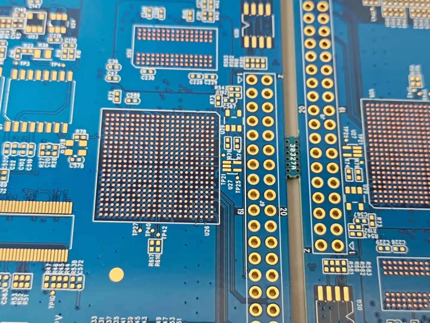
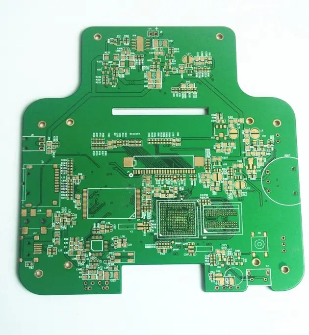
DeSPIte its advantages, double-sided boards are not the best construction method, especially for sensitive or high-speed circuit design. Therefore, for high-speed design, we usually use multilayer boards. The most common board thickness is 1.6 mm, the material is FR-4, and there are independent GND or POWER layers. There are many PCB design issues that need to be paid attention to for multilayer boards. Here are some obvious reasons for using multilayer Board Design:
It has independent power and ground connection wiring layer. If the power supply is also on a plane, other identical power networks can be connected together by simply adding vias.
Other layers can be used for signal wiring, which can provide more routing space for wiring.
There will be distributed capacitance between the power supply and the ground plane to reduce high-frequency noise.
However, other reasons for multilayer boards may not be obvious or intuitive, mainly including the following two points:
Better EMI/RFI suppression. Because of the image plane effect, it has been known since the Marconi era. When the conductor is placed close to the parallel conductive surface, most of the high-frequency current will return directly below the conductor and flow in the opposite direction. The mirror image of the conductor in the plane forms the transmission line. Since the current in the transmission line is equal and opposite, it is relatively unaffected by radiated noise. Instead, the signals are coupLED very efficiently. Image plane effects are as effective as ground and power planes, but they must be continuous. Any gap or discontinuity will lead to the rapid disappearance of beneficial effects.
Reduce overall project costs for SMAll volume production. Although the manufacturing cost of multilayer boards is high, the EMI/RFI requirements of FCC or other institutions may require expensive testing of the design. If there is a problem, you may need to push it down to redesign the PCB for additional testing. Compared with 2-layer PCB, the EMI/RFI performance of multilayer PCB can be improved by 20 dB. If the output is small, it is meaningful to design better PCB first.
Effectively prevent crosstalk between various signal layers.
The production process requirements are relatively high. Compared with the 2-layer board design, it is not so difficult.


抖音二維碼

Q Q二維碼

微信二維碼
點(diǎn)擊
然后
聯(lián)系
然后
聯(lián)系
電話熱線
13410863085Q Q

微信

- 郵箱