鑫景福致力于滿足“快速服務,零缺陷,輔助研發”PCBA訂購單需求。


行業新聞
What are the different functions of gold plating and silver plating on PCB
Many DIY players will find that PCB colors used by various board products in the MARKet are dazzling. The common PCB colors are black, green, blue, yellow, purple, red, and brown.
In addition, some manufacturers have developed PCB with different colors such as white and pink.
In the traditional impression, the black PCB seems to be positioned at the high-end, while the red and yellow PCBs are dedICated to the low-end. Is that so?
1. PCB copper layer without solder mask is very easy to oxidize when exposed to air
We know that both sides of a PCB are copper layers. In the production of PCB, whether the copper layer is made by addition or subtraction, it will get a smooth and unprotected surface.
Although the chEMIcal properties of copper are not as active as aluminum, iron, magnesium, etc., pure copper is easily oxidized in contact with oxygen in the presence of water; Because there are oxygen and water vapor in the air, the surface of pure copper will undergo oxidation reaction soon after contacting with the air.
Because the copper layer in PCB is very thin, the oxidized copper will become a bad conductor of electricity, which will greatly damage the electrical performance of the entire PCB.
In order to prevent copper oxidation, separate the welding part and non welding part of PCB during welding, and protect the surface layer of PCB, engineers invented a special coating. This coating can be easily brushed on the surface of PCB to form a protective layer with a certain thickness and block the contact between copper and air. This coating is calLED solder mask, and the material used is solder mask.
Since it's called lacquer, there must be different colors. Yes, the original solder mask can be made colorless and transparent, but for the convenience of maintenance and manufacturing, PCB often needs to print SMAll words on the board.
Transparent solder resist paint can only show the bottom color of PCB, so the appearance is not good enough for manufacturing, maintenance or sales. Therefore, engineers add various colors to the solder resist paint to form a black or red or blue PCB.
2. The black PCB is difficult to see the wiring, which makes maintenance difficult
From this point of view, the color of PCB has nothing to do with the quality of PCB. The difference between black PCB and blue PCB, yellow PCB and other color PCBs lies in the color of solder resist paint painted on them.
If the PCB design and manufacturing process are exactly the same, the color will not have any impact on the performance or heat dissipation.
As for the black PCB, its surface routing is almost completely covered, causing great difficulties for later maintenance, so it is a color that is not convenient for manufacturing and use.
Therefore, in recent years, people have gradually reformed, giving up the use of black solder resist paint, and using dark green, dark brown, dark blue and other solder resist paints, in order to facilitate manufacturing and maintenance.
At this point, we have basically understood the problem of PCB color. As for the statement of "color represents or low-end", it is because manufacturers prefer to use black PCB to manufacture high-end products and use red, blue, green, yellow, etc. to manufacture low-end products.
To sum up, products are endowed with color meanings, not colors.
3. What are the advantages of using gold, silver and other precious metals on PCB?
The color is clear, and then talk about the precious metals on PCB! When some manufacturers promote their products, they will specially mention that their products have adopted special processes such as gold plating and silver plating. So what's the use of this process?
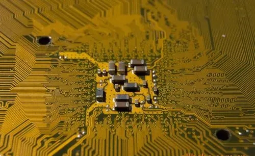
When PCB surface needs to weld components, it is required that a part of copper layer is exposed for welding. These exposed copper layers are called bonding pads. The bonding pads are generally rectangular or round, with a small area.
In the above, we know that the copper used in PCB is very easy to be oxidized, so the copper on the pad will be exposed to the air after brushing the solder mask.
If the copper on the pad is oxidized, it is not only difficult to weld, but also the resistivity increases greatly, which seriously affects the performance of the final product. Therefore, engineers have come up with various methods to protect pads. Such as plating inert metal gold, or coating a layer of silver on the surface by chemical process, or covering copper with a special chemical film to prevent the pad from contacting with the air.
The copper layer of the bonding pad exposed on the PCB is directly exposed. This part needs protection to prevent it from being oxidized.
From this point of view, the purpose of the process itself is to prevent the bonding pad from being oxidized, protect the bonding pad, and ensure its yield in the next welding process, regardless of whether it is gold or silver.
However, the use of different metals will require the storage time and conditions of PCB used in the production plant. Therefore, PCB manufacturers generally use vacuum plastic packaging machines to package PCB after PCB production is completed and before it is delivered to customers for use, so as to ensure no oxidative damage to PCB.
Before the components are welded on the machine, the board manufacturer also needs to detect the oxidation degree of PCB, remove the oxidized PCB, and ensure the yield. The boards obtained by the end consumers have passed various tests. Even if they are used for a long time, the oxidation will almost only occur in the plug-in connection parts, and there is no impact on the pads and the components that have been welded.
Since the resistance of silver and gold is lower, will the use of special metals such as silver and gold reduce the heating of PCB?
We know that the factor affecting the heat generation is resistance; The resistance is also related to the material, cross-sectional area and length of the conductor itself. The thickness of the metal material on the pad surface is even far less than 0.01 mm. If the pad is treated with OST (organic protective film), there will be no excess thickness. The resistance displayed by such a small thickness is almost 0, which can not even be calculated, and certainly will not affect the heat generation.
PCB manufacturers, PCB designers and PCBA manufacturers will explain to you the different functions of gold plating and silver plating on PCB.


抖音二維碼

Q Q二維碼

微信二維碼
點擊
然后
聯系
然后
聯系
電話熱線
13410863085Q Q

微信

- 郵箱