鑫景福致力于滿足“快速服務,零缺陷,輔助研發”PCBA訂購單需求。


行業新聞
Solution to Negative Film Deformation in PCB process
Cause and Solution PCB Technology Negative Film Deformation
reason:
(1) Poor temperature and humidity control
(2) The temperature of the exposure machine rises too high
Solution:
(1) Generally, the temperature is controlLED at 22 ± 2 ° C and the humidity is controlled at 55% ± 5% RH.
(2) Use cold light source or aerator with cooling devICe, and constantly replace the spare membrane
Negative film deformation solution of PCB technology
Negative film distortion correction process:
1. Change the hole bit method
Under the condition of mastering the operation technology of the digital program designer, first compare the negative film with the drilling test board to measure the two deformations of length and width.
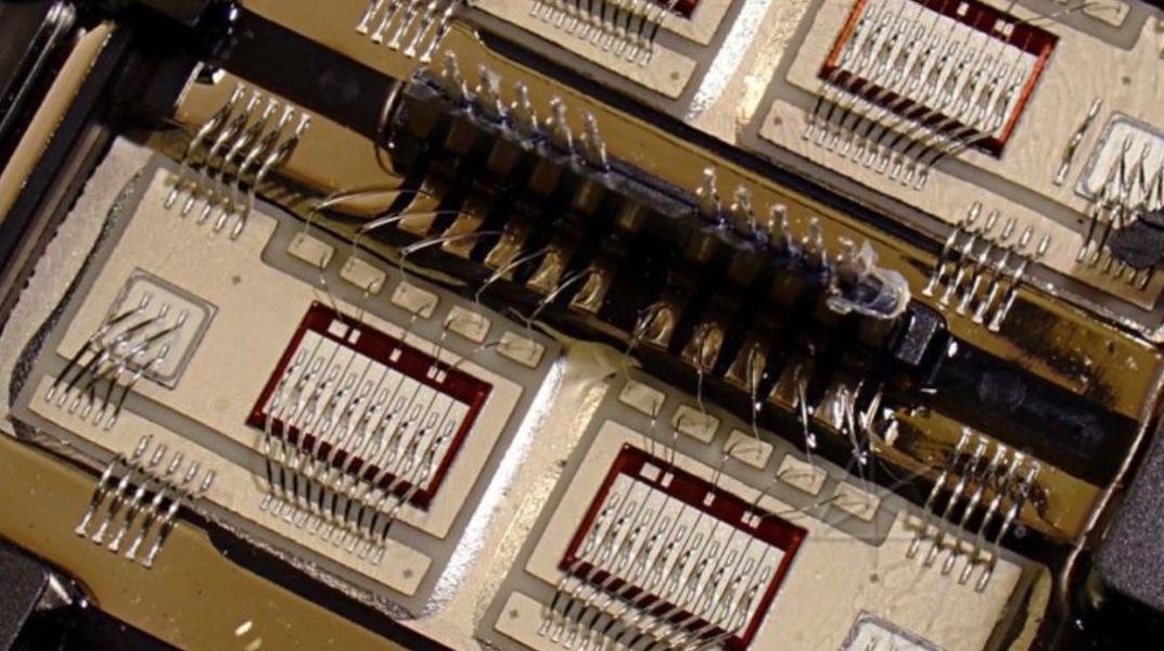
Circuit board

For the digital program designer, the hole position is lengthened or shortened according to the deformation amount, and the drilling test plate with lengthened or shortened hole position is used to adapt to the deformed negative film This method eliminates the tedious work of splicing films and ensures the integrity and accuracy of graphics
2. Suspension method
In view of the physical phenomenon that the negative will change with the change of ambient temperature and humidity, before copying the negative, put the negative into a sealed bag and hang it under the working environment for 4-8 hours to deform the negative before copying. Make the film SMAller after copying.
3. For patterns with SIMple lines, large line width, large spacing and irregular deformation, the deformed part of the negative film can be cut off, and then re spliced on the hole bit of the drilling test plate before copying
4. PCB pad overlapping method
Use the holes on the test board to expand it to the size of the pad, and remove the deformed segments to ensure the minimum loop width technical requirements.
5. Texture method
Scale up the graphics on the deformation film and reposition the printing plate
6. Shooting method
Use the CAMera to zoom in or out of the deformed shape.
Negative film deformation solution of PCB technology
Description of these relevant methods
1. Splicing method:
Application: The coating lines are not dense, and the deformation of each layer is inconsistent; Especially suitable for welding mask and multi-layer power supply grounding film deformation;
Not applicable: the linear density of negative film is high, and the line width and spacing are less than 0.2mm;
Note: When cutting, please reduce the damage to the wire as much as possible, and do not damage the gasket. When splicing and copying, attention should be paid to the correctness of the connection relationship.
2. How to change the hole bit:
Application: The deformation of each layer is consistent. Line dense negatives are also suitable for this method.
Not applicable: The film deformation is uneven, and the local deformation is particularly serious.
Note: After using the program designer to extend or shorten the hole position, the tolerance hole position should be reset.
3. Suspended piping:
Applicable film that is not deformed and prevents deformation after copying;
Not applicable: deformed negative film.
Note: Dry the film in a ventilated and dark environment to avoid contamination. Ensure that the air temperature is the same as the temperature and humidity of the workplace.
4. Bonding pad lapping method
Scope of application: The graphic lines should not be too dense, and the line width and spacing should be greater than 0.30mm;
Not applicable: In particular, users have strict requirements on the appearance of printed circuit boards;
Note: After overlapping, the PCB pad is oval, and the lines and halo on the pad edge are easy to deform.
5. How to take pictures
Application: PCB film has the same deformation rate in the length and width directions If it is not convenient to use the heavy drilling test plate, only the silver salt film can be used
N/A: The length and width of the film are deformed differently.
Note: When shooting, focus should be accurate to prevent distortion of lines. The film lost a lot. In general, several adjustments must be made to obtain a satisfactory circuit pattern.
The above is the explanation given by the editor of pcb circuit board company.
If you want to know more about PCBA, you can go to our company's home page to learn about it.
In addition, our company also sells various circuit boards,
High Frequency Circuit Board and SMT chip are waiting for your presence again.


抖音二維碼

Q Q二維碼

微信二維碼
點擊
然后
聯系
然后
聯系
電話熱線
13410863085Q Q

微信

- 郵箱