鑫景福致力于滿足“快速服務,零缺陷,輔助研發”PCBA訂購單需求。


行業新聞
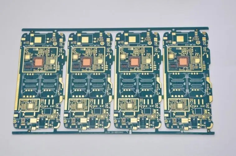
How to view SMT chip inspection and circuit board segmentation
This step of SMT patch inspection can standardize the process quality requirements of SMT processing to ensure that the product quality meets the requirements. Now let's take a look at the SMT patch inspection standards?
1、 SMT chip solder paste process
1. The tin spraying position printed on the PCB shall be centered with the bonding pad, without obvious deviation, whICh shall not affect the pasting and tinning effect of SMT components.
2. The amount of tin sprayed on the PCB is moderate, and the solder pad cannot be completely covered, with less tin and missing brush.
3. The printing tin spraying point on the PCB is poorly formed, the printing tin spraying is connected with tin, and the tin spraying is concave and uneven, and the tin spraying displacement exceeds one third of the bonding pad.
2、 SMT patch red glue process
1. The position of the red printing glue is in the middle, without obvious deviation, which can not affect the pasting and soldering.
2. The amount of printing red glue is moderate, which can be pasted well without insufficient glue.
3. The red glue dot of printing is offset between two pads, which may cause difficulty in tinning components and pads.
4. The amount of red printing glue is too much, and the width of glue seeping from the underside of the component body side is greater than half of the width of the component body.
3、 SMT mounting process
1. SMT components shall be instalLED in order, in the middle, without deviation and skew.
2. The model and specification of SMT components at the mounting position should be correct, and the components should be reversed. The components are pasted reversely (it is not allowed to interchange the positions of two opposite sides of the components with differences, such as the upside down side of the side with silk screen MARK and the side without silk screen mark), so the function cannot be realized.
3. The mounting of SMD components with polarity requirements shall be processed according to the correct polarity marks. The device polarity is pasted reversely and wrongly (diode, triode, tantalum capacitor).
4. Soldering pads of multi pin devices or adjacent components shall be free of tin connection and bridging short circuit.
5. Solder pads of multi pin devices or adjacent components shall be free of residual solder beads and dross.
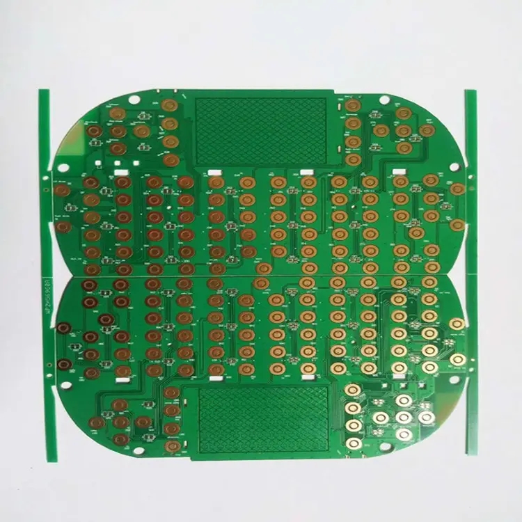
Two Kinds of circuit board Segmentation Methods and Multilayer Circuit Board Segmentation Methods
Division refers to dividing the whole or related things into two or more pieces. Circuit board segmentation refers to dividing a circuit board into two or more pieces according to a reasonable circuit without affecting its effectiveness. PCB segmentation is usually performed by using a PCB splitter. Reasonable PCB segmentation is conducive to the secondary processing, recycling and remanufacturing of PCB. The circuit board division also has a great impact on the development of the circuit board industry
Next, we will introduce two PCB segmentation methods and multi-layer PCB segmentation methods
PCB division mode
Division method 1
The signal line crosses the gap between the two grounds. What is the return path of the signal current? It is assumed that the two divided grounds are connected at some place (usually at a single point at a certain position). In this case, the ground current will form a large loop, and the high-frequency current flowing through the large loop will generate radiation and high inductance.
If the low level analog current flows through the large loop, the current is easily interfered by external signals. When the split ground is connected together at the power supply, a very large current loop will be formed. In addition, analog ground and digital ground are connected together by a long wire to form a DIPole antenna.
The key to optimize the mixed signal circuit board design is to understand the path and mode of current return to ground. When most designers design circuits, they often ignore the specific path of the circuit and only consider where the signal current flows. If the division of the ground wire layer must be routed through the gap between the divisions, a single point connection can be made between the divided ground to form a connection bridge between the two grounds, and then the wiring can be routed through the connection bridge. In this way, a direct current return path can be provided below each signal line, so that the formed loop area is very SMAll.
The optical isolation device or transformer can also be used to realize the signal crossing the separation gap. For the former, it is the optical signal that spans the segmentation gap; For latecomers, it is the magnetic field that crosses the gap. Another feasible method is to use differential signal: the signal flows from one signal line and returns from another signal line. In this case, the ground does not need to be used as the return path.
Division method 2
In practical work, PCB is generally divided into analog part and digital part. Analog signals are routed in the analog area of all layers of the circuit board, while digital signals are routed in the digital circuit area. In this case, the return current of the digital signal will not flow to the ground of the analog signal,
The reason for the interference of digital signals to analog signals is that the wiring of digital signals is not appropriate. For example, the digital signal is wired on the analog part of the circuit board, or the analog signal is wired on the digital part of the circuit board. This is not because there is no division.
PCB board is designed in a unified way. Through digital circuit and analog circuit zoning and proper signal wiring, it can usually solve some more complex layout and wiring problems, and it will not cause some potential troubles due to ground segmentation. In this case, the layout and partition of components become the key to determine the design quality.
If the layout and wiring are reasonable, the digital ground current will be limited to the digital part of the circuit board and will not interfere with the analog signal. Such wiring must be carefully checked and checked to ensure compliance with the wiring rules, otherwise, improper routing of a signal wire will completely destroy the design of the entire circuit board.
The above are the methods for most PCB segmentation. Now let's introduce the specific segmentation methods for multi-layer PCB segmentation
How to divide the middle layer setting and the inner electric layer of multilayer circuit board
The difference between multilayer circuit boards and general circuit boards is that in addition to the general top and bottom layers, multilayer circuit boards also have several intermediate layers, which can be signal layer or internal power/ground plane. Next, we will introduce how to create and set an intermediate layer for multilayer boards, and how to segment the electrical layer in Multilayer boards.
1. Creation and setup of middle layer of multilayer circuit board
The function of the middle layer of the multilayer board is SIMilar to that of the top and bottom layers, except that components cannot be placed. The internal power supply/ground plane is a layer of copper film, which can be divided into mutually isolated areas. Each area of copper film is connected with a specific power supply/ground network through pads or vias. Its role is to simplify the connection between the power supply and the bottom grid, reduce the line impedance, and enhance the anti-interference capability of the power supply network.
The creation method of the middle layer can be realized through the special layer setting and management tool layer stack manager. The specific operation is to select the menu command [Design]/[Layer Stack Manager]. You can easily set the required layer in the pop-up dialog box. Take the four layer board as an example. The two middle layers are respectively the power layer (power) and the ground layer (gnd). The connected network number is not set. It is worth noting that for the four layer board, the general way to select layers is signal layer, power layer, layer and signal layer. The better way to select layers is signal layer, power layer, signal layer and stratum.
2. A method of electrical layer segmentation in multilayer circuit board
After the intermediate layer is planned and set, the internal power layer can be divided after the component layout is completed. The internal power layer division of protel dxp 2004 is much simpler and more convenient than the previous version. For the specific operation method, select the menu command [Design]/[PCB layer color] or directly press the shortcut letter key l to call up the [Board Layer and Color] panel, so that you can turn off unwanted layers (such as the top layer, bottom layer, and other intermediate layers) and display the desired partition layer. Take the power layer as an example, check the power layer [power] to display the "power" layer on the PCB interface. Back to the PCB operation interface, select the menu command [Place]/[Line] or shortcut key p/l to call up the line drawing tool. Select the power pad to be divided (such as vcc) to form a closed surface. Double click the closed box to pop up a dialog box and select the network (vcc) connected to the closed area divided. A divided internal power layer has been completed, and the operation of other power supply networks (vdds) is similar.
PCB manufacturers, PCB designers and PCBA manufacturers will explain how to view SMT chip inspection and PCB segmentation.


抖音二維碼

Q Q二維碼

微信二維碼
點擊
然后
聯系
然后
聯系
電話熱線
13410863085Q Q

微信

- 郵箱