鑫景福致力于滿足“快速服務,零缺陷,輔助研發”PCBA訂購單需求。


行業新聞
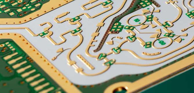
Problems in Manufacturing multilayer printed circuit boards
In short, printed circuit boards, also known as PCBs, enable all Electronic devices to operate as expected Therefore, when there is a problem with the printed circuit board ElectronIC equipment may not function as expected printed circuit board problems are a major challenge for manufacturers because many things go wrong Especially in multilayer PCB manufacturing process The following lists 7 problems in the manufacturing process of multilayer PCB
By understanding these problems, as a designer, you will consider these problems when building a printed circuit board, hoping to avoid these problems and subsequently damage the printed circuit board.
Design
Problems related to bending and twisting may occur when designing multilayer printed circuit boards. Bending and twisting are some of the most common features used to determine PCB flatness. Arc is the cylindrical or spherical curvature of a printed circuit board. On the other hand, deformation occurs when the deformation is parallel to the diagonal of the printed circuit board.
There are several steps for a multi-layer correct PCBservice provider. Fortunately, there are various PCB manufacturing companies that can take steps to avoid bending and twisting. First, multilayer PCB manufacturers need to use appropriate parameters when pressing multilayer PCB to reduce the stress on PCB. Second, they need to avoid mixing data from multiple vendors. Third, the data used should comply with RoHS guidelines. As a PCB manufacturer, you also need to use or use a horizontal oven during the curing process to avoid problems related to PCB bending and twisting.
Pressing multilayer PCB
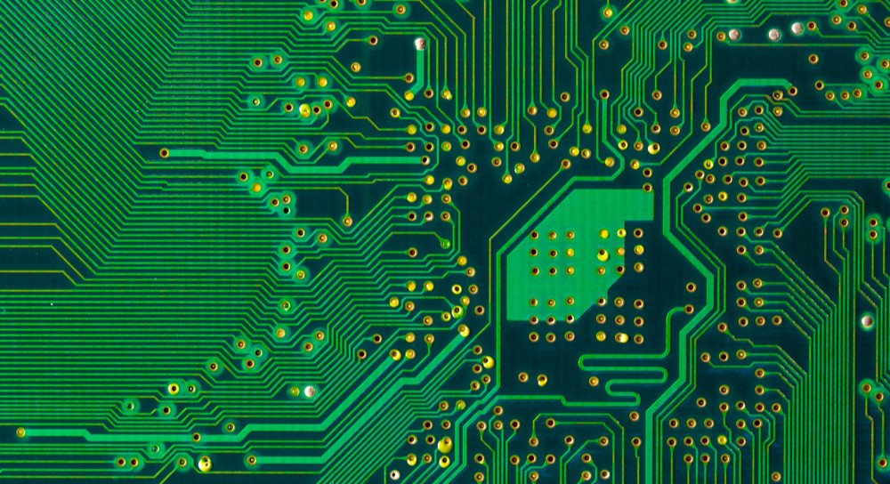
Circuit board

Multilayer printed circuit board refers to a printed circuit board that contains multiple single-layer counts, which need to be stacked Laminate is to lay out the insulating layer and the copper layer before the PCB
In the manufacturing of multilayer printed circuit boards, it is a challenge to laminate the insulating layer and copper together. Most multilayer PCB manufacturers often encounter difficulties in pressing components of multilayer PCB together.
In order to ensure the smooth stacking process of multilayer printed circuit boards, in addition to using the best laminating information, manufacturers need to ensure that they use the machine most suitable for this work.
Selection of matrix
Printed circuit board materials have two basic uses. First, they conduct electricity, and second, they provide insulation between conductive copper layers. It is easy to understand that the selection of substrate information is critical to the success of PCB. In addition to affecting the thermal behavior of PCB. The files you use on a PCB also affect the mechanical and electrical characteristics of the PCB.
1. Dielectric constant
Because most PCB functions are determined by the substrate information. This means that the substrate data with high-frequency characteristics need to be applied to high-frequency and high-Speed PCBs. However, high frequency substrate data must satisfy SMAll and stable dielectric constants.
2. Matrix characteristics
In addition, the substrate must perform well in terms of heat resistance. Stability, impact strength, chEMIcal resistance and manufacturability. It is important to ensure that the substrate data used for high-speed and high-frequency printed circuit boards must have low moisture absorption or be composed of low moisture absorption. Copper foil also needs to meet high peel strength.
3. Insulation
FR4, also known as FR-4, is one of the most versatile low-cost multilayer substrate materials and is known for providing excellent performance. FR-4 data provide some optimal electrical insulation with high dielectric strength.
Multilayer PCB manufacturing Resin infiltration manufacturing
Resin plug process is the standard process in the whole PCB industry, especially in high-frequency products requiring large thickness and high count. In recent years, the application of resin sealing technology is more and more extensive, and has been widely used in HDI panels. If you want to solve or eliminate the problems that cannot be solved by pressure filling or green oil plugging resin, it is better to use resin for plugging.
Resin plugging is a problem faced by most manufacturers when manufacturing multilayer printed circuit boards. However, the best way to solve this problem is to use a vacuum stopper.
Resin plugging is a preventive measure to ensure that the through-hole is protected from accidental solder flow, especially during welding and assembly. The main use of resin, especially in the manufacture of printed circuit boards, is to clamp fibers together to protect them from external factors.
Manufacturing of dense cooling holes
When manufacturing printed circuit boards, you may encounter problems related to heat dissipation. Heat dissipation is a method of heat transfer. Heat dissipation occurs when objects that are hotter than other uses are placed or placed in the environment where the heat from hotter parts is transferred to cooler objects. Heat dissipation occurs in many ways, mainly through convection, conduction and radiation.
The problems related to heat dissipation are faced by many printed circuit board manufacturers. However, in order to eliminate intensive heat dissipation, it is better to use the best or recommended heat dissipation materials, such as aluminum.
Backdrilling production of multi-layer PCB manufacturing
Backdrilling is one of the best manufacturing technologies. It is usually used for a large number of high-speed multilayer printed circuit boards to reduce or minimize the parasitic effect of electroplated through-hole. Backdrilling, also known as controlLED depth drilling, is a technology that allows you to remove some unused parts, stubs, and copper tubes from through holes on the circuit board of a printed circuit board.
In addition to improving signal integrity and reducing the difficulty of manufacturing PCB, the back drilling also reduces the noise interference to PCB. When it coMES to the manufacturing of multilayer printed circuit boards. Backdrilling is a major challenge for many manufacturers. Some of the most likely backdrilling challenges include hole cleaning. Barite depression, pipe sticking, loop loss and phyllite instability.
Multilayer PCB manufacturing test
In the PCB development cycle, the test phase of the printed circuit board is an indispensable part. In the whole PCB manufacturing process. Testing printed circuit boards can help save money and prevent problems or difficulties in the final production run.
Unfortunately, when multi-layer manufacturing is involved Most PCB manufacturing companies failed to use the best PCB testing method Some of the best and recommended PCB tests are bare board tests, online tests, functional tests, and assembly level tests Testing, especially multilayer PCB, can identify any technical defects in PCB


抖音二維碼

Q Q二維碼

微信二維碼
點擊
然后
聯系
然后
聯系
電話熱線
13410863085Q Q

微信

- 郵箱