鑫景福致力于滿足“快速服務,零缺陷,輔助研發”PCBA訂購單需求。


行業新聞
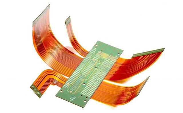
What is the internal structure of multilayer circuit board
The Circuit board manufacturer, circuit board designer and PCBA manufacturer explain to you the internal structure of multi-layer circuit boards
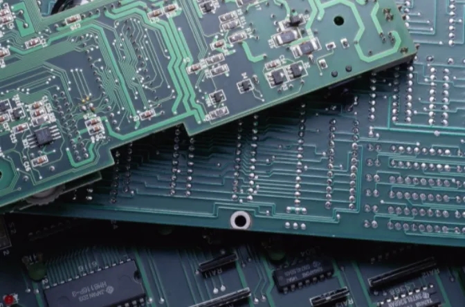
When a hardware engineer first touches a multilayer PCB, it is easy to see faint. The lines are like SPIder webs.
Several internal structure diagrams of multilayer PCB circuit board are drawn, and the internal structure of PCB diagrams of various stack structures are displayed with stereo graphICs.
The core of HDI is via
The circuit processing of multilayer PCB is no different from that of single-layer and double-layer PCB. The biggest difference lies in the via process.
The lines are etched, and the vias are drilLED and plated with copper. We all understand these hardware developments, so we won't repeat them.
multilayer circuit boards usually include through hole boards, first order boards, second order boards, and second order perforated boards. Higher order boards, such as third-order boards and interconnection boards at any layer, are seldom used, and the price is expensive. I won't discuss it more.
Generally, 8-bit MCU products use 2-layer through-hole boards; The intelligent hardware of 32-bit single chip microcomputer level uses 4-6-layer through-hole boards; Linux and Android level intelligent hardware, using 6-tier through-hole to 8-tier HDI boards; Compact products such as SMArt phones generally use 8-layer 1-level to 10 layer 2-level circuit boards.
The most common through hole
There is only one kind of via, from the first layer to the last layer. Whether it is an external circuit or an internal circuit, holes are punched through, which is called a through-hole plate.
The number of layers has nothing to do with the through-hole board. Usually, the 2-layer through-hole board is used by everyone, while many switches and military circuit boards are made of 20 layers of through-hole boards.
Drill through the circuit board with a drill, and then plate copper in the hole to form a path.
It should be noted here that the inner diameters of through-hole are usually 0.2mm, 0.25mm and 0.3mm, but generally 0.2mm is much more expensive than 0.3mm. Because the drill bit is too thin and easy to break, it is also slow to drill. The cost of more time and drill bit is reflected in the rise in the price of circuit boards.
Laser hole of high density board (HDI board)
Layered structure diagram of 6 layers of 1st order HDI board. The two layers on the surface are laser holes with an inner diameter of 0.1mm. The inner layer is a mechanical hole, which is equivalent to a 4-layer through-hole plate, and the outer layer is covered with 2 layers.
The laser can only penetrate glass fiber plates, not metal copper. Therefore, the external surface drilling will not affect other internal lines.
After laser drilling, copper plating is performed to form laser vias.
Two layer laser hole of 2nd order HDI board
It is a 6-layer 2-step staggered hole HDI board. Usually, people use 6 floors and 2 levels less, mostly from 8 floors and 2 levels. There are more layers here, which is the same as the six layers.
The so-called second order is that there are two layers of laser holes.
The so-called staggered hole means that two layers of laser holes are staggered.
Why should they be staggered? Because the copper plating is not enough, the hole is empty, so you can not directly re drill on it. You should stagger a certain distance, and then make another layer of empty.
The second level of the sixth floor=two layers outside the first level of the fourth floor.
The second level of the eighth floor=the first level of the sixth floor plus two layers.
The process of orifice plate is complex and the price is higher
The two laser holes of the staggered hole plate are overlapped. The line will be more compact.
The inner laser hole needs to be plated and filled, and then the outer laser hole needs to be made. The price is more expensive than the wrong hole.
Ultra expensive multilayer laser hole stacking for arbitrary layer interconnection board
That is, each layer is a laser hole, and each layer can be connected together. You can route the wire as you want, and punch holes as you want.
Layout engineer thinks it's cool! No longer afraid of painting!
The purchaser wants to cry when he thinks about it. It is more than 10 tiMES more expensive than ordinary through-hole boards!
Therefore, only products like iPhone can be used. For other mobile phone brands, I have never heard of anyone who has used any layer of interconnection board.
summary
Finally, put a picture and compare it carefully.
Please note the size of the observation hole and whether the pad of the hole is closed or open.
PCB manufacturers, PCB designers and PCBA manufacturers will explain to you the internal structure of multi-layer PCB.


抖音二維碼

Q Q二維碼

微信二維碼
點擊
然后
聯系
然后
聯系
電話熱線
13410863085Q Q

微信

- 郵箱