鑫景福致力于滿足“快速服務,零缺陷,輔助研發”PCBA訂購單需求。


行業新聞
SpecifICation of PCB silk screen and classification of PCB through-hole
PCB manufacturers, PCB designers and PCBA processors will explain the PCB silk screen specifications and the classification of PCB through-hole
PCB silk screen is an important process in PCB manufacturing, which also determines the quality of finished PCB. What are the specifications and requirements for screen printing of PCB?
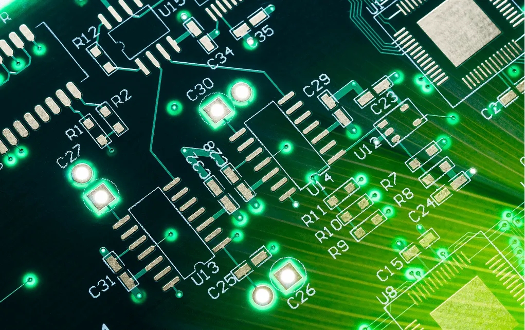
All components, mounting holes and positioning holes have corresponding silk screen labels. In order to facilitate the installation of finished boards, H1, H2...... Hn is used to identify the mounting hole silk screen on the PCB.
2. The silk screen characters shall follow the principle of from left to right and from bottom to top as far as possible; For polar devices such as electrolytic capacitors and diodes, keep the same direction in each functional unit as far as possible.
3. There is no silk screen on the device bonding pad and tin path that needs tin coating, and the device tag number should not be covered by the device after installation; The silk screen shall not be pressed on the through hole and bonding pad to avoid the loss of part of the silk screen when the resistance welding window is opened; The screen spacing is greater than 5mil.
4. For polar components, their polarity shall be clearly indicated on the silk screen diagram, and the polarity direction MARK shall be easy to identify.
5. The direction of the connector with direction is clearly indicated on the silk screen.
6. If the space on the PCB surface allows, the PCB shall be provided with a barcode silk screen frame, and the position of the barcode shall be convenient for scanning.
7. PCB documents shall have screen prints of board information such as board name, date and version number, with clear and striking positions.
8. The PCB shall have complete relevant information and anti-static identification of the manufacturer.
9. The number of PCB photo files is correct, each layer should have correct output, and there should be complete layer output.
10. The identifier of components on PCB must be consistent with that in BOM list.
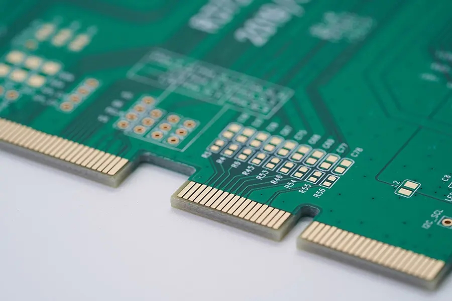
Classification of PCB through holes
Through hole is the most common hole in PCB, which mainly plays the role of connecting and conducting circuits. Next, let the engineer share with you the classification of PCB through-hole.
Through holes are traditionally classified into electroplated (supported) holes and non electroplated (unsupported) holes. This is a manufacturing term. For design, holes should be divided into two categories: those that are welded and those that are not welded.
1. Through hole to be welded.
Except that the external surface area must be large to enhance heat dissipation to avoid poor welding, most of the rules are applicable to the welded through-hole. For consistency and ease of calculation, the inner pad should be the same as the outer pad unless SIMplified pads are required
2. Through hole not to be welded.
The designer must first know whether the pad is confirmed to be welded or not. This information helps engineers decide whether the pad is calculated for welding or for the SMAllest hole ring. It is important to note that the pad is plated or not electrified. In the electroplating process, if the pad exists, the hole should be plated with copper foil. If the pad is not plated, it must be drilLED after the plating process.
(1) Non plated through-hole, with pad
Non plated through-hole means that there is no plating in the hole passing through the pad. This means that except for the normal copper adhesive, there is no additional carrier to support the pad. For this reason, pads must be large enough to bond and support pads during heating or welding.
(2) Non plated through-hole, no pad
The universal NPTH is as large as the plated hole without pad or hole wall on a printed board, such as mounting hole, screw adjustment access hole, wire transfer hole, etc. Non electroplating or hole ring requirements are necessary, and the universal through-hole is different from other holes, because it has no electroplating or soldering considerations.
PCB manufacturers, PCB designers and PCBA processors will explain the PCB silk screen specifications and the classification of PCB through-hole.


抖音二維碼

Q Q二維碼

微信二維碼
點擊
然后
聯系
然后
聯系
電話熱線
13410863085Q Q

微信

- 郵箱