鑫景福致力于滿足“快速服務(wù),零缺陷,輔助研發(fā)”PCBA訂購單需求。


行業(yè)新聞
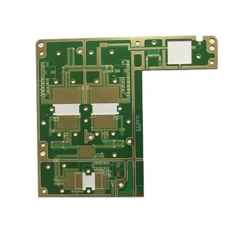
The PCB manufacturer explains why PCB manufacturers need test points
PCB manufacturers, PCB designers and PCBA manufacturers explain why PCB manufacturers need test points
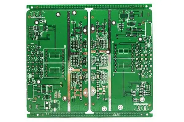
The PCB factory basICally sets test points to test whether the components on the circuit board meet the specifications and solderability. For example, if you want to check the resistance of a circuit board, the SIMplest way is to measure its two ends with a multimeter.
However, in mass production factories, there is no way for you to slowly measure each resistance, capacitance, inductance, and even IC circuit on each board with an electric meter. Therefore, the so-calLED ICT (In Circuit Test) automatic testing machine appears. It uses multiple probes (commonly called "Bed Of Nails" fixtures) to contact all the parts and circuits on the board that need to be measured at the same time, Then, the characteristics of these electronIC parts are measured in sequence through program control, mainly in sequence, supplemented by juxtaposition. Generally, the test of all parts of a general board can be completed in about 1-2 minutes. Depending on the number of parts on the circuit board, the more parts, the longer the time.
However, if these probes directly contact the electronic parts or their welding legs on the board, it is likely to crush some electronic parts, which is counterproductive. Therefore, there is a test point. An additional pair of round dots are introduced at both ends of the part. There is no mask on it. The test probe can contact these dots without directly contacting the measured electronic parts.
In the early days when the circuit board was still a traditional plug-in (DIP), it was true that the solder legs of parts were used as test points, because the solder legs of traditional parts were strong enough to not be afraid of pin pricking, but the misjudgment of poor probe contact often occurred, because after wave soldering or SMT tin eating, a layer of residual film of solder paste flux was usually formed on the solder surface of general electronic parts, The impedance of this film is very high, which often leads to poor contact of the probe. Therefore, it is often seen that the test operators of the production line often blow hard with an air spray gun, or wipe these places that need to be tested with alcohol.
In fact, the probe may have poor contact at the test point after wave soldering. Later, after the prevalence of SMT, the situation of test misjudgment has been greatly improved, and the application of test points has also been given a great responsibility. Because SMT parts are usually fragile and cannot withstand the direct contact pressure of the test probe, the use of test points allows the probe to not directly contact the parts and their weld legs, which not only protects the parts from damage, but also indirectly greatly improves the reliability of the test, because there are fewer misjudgments.
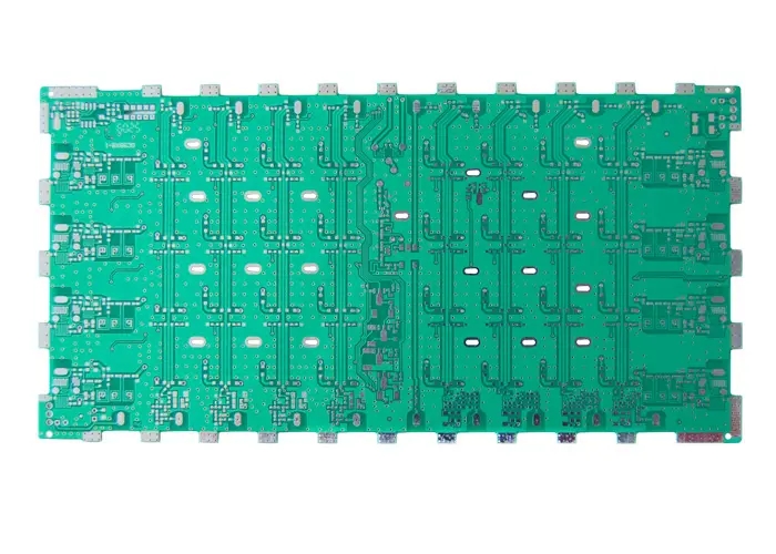
However, with the development of science and technology, the size of the circuit board is getting SMAller and smaller. It is hard to squeeze so many electronic parts on a Small circuit board. Therefore, the problem that the test point occupies the space of the circuit board often leads to a tug of war between the design end and the manufacturing end. The appearance of the test point is usually round, because the probe is also round, which is easier to produce, and it is easier to make adjacent probes closer, so that the needle planting density of the needle bed can be increased.
There are some limitations on the mechanism when using a needle bed for circuit testing. For example, the minimum diameter of the probe has a certain limit. A needle with too small diameter is easy to break.
The distance between needles is also limited, because each needle must come out of a hole, and a flat cable must be welded at the back end of each needle. If the adjacent holes are too small, in addition to the problem of contact short circuit between needles, the interference of flat cables is also a big problem.
Some high parts cannot be planted with needles. If the probe is too close to the high part, there will be a risk of damage caused by collision with the high part. In addition, because the part is high, it is usually necessary to make holes on the needle bed of the test fixture to avoid it, which also indirectly causes that the needle cannot be planted. Test points of all parts on the circuit board that are increasingly difficult to accommodate.
As the boards are getting smaller and smaller, the number of test points has been discussed repeatedly. Now there are some methods to reduce test points, such as Net test, Test Jet, Boundary Scan, JTAG, etc; There are also other test methods that want to replace the original needle bed test, such as AOI and X-Ray, but at present, each test seems unable to replace ICT 100%. PCB manufacturers, PCB designers and PCBA manufacturers will explain to you why PCB manufacturers need test points for PCB boards.


抖音二維碼

Q Q二維碼

微信二維碼
點擊
然后
聯(lián)系
然后
聯(lián)系
電話熱線
13410863085Q Q

微信

- 郵箱