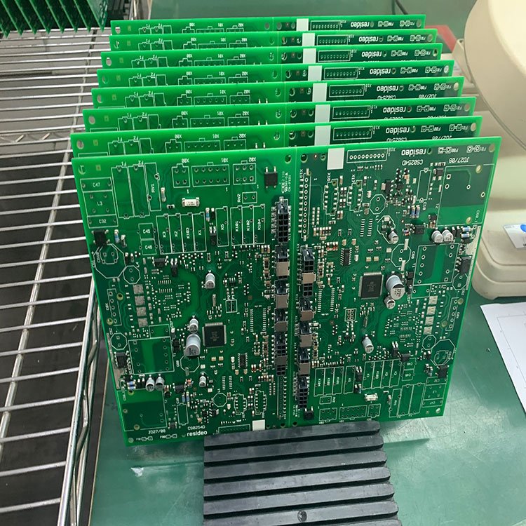
鑫景福致力于滿足“快速服務(wù),零缺陷,輔助研發(fā)”P(pán)CBA訂購(gòu)單需求。


行業(yè)新聞
Explain the warping, arching, twisting and sagging of PCB
PCB manufacturers, PCB designers and PCBA processors explain the warping, arching, twisting and sagging of PCB
What are plate warping, arching, twisting and sagging?
circuit board warping is an unexpected change in the geometry of a printed circuit board (PCB). The circuit board warping is a general term used to describe the changed PCB shape, independent of the shape itself (bow, twist, etc.). One of the main challenges in dealing with warped plates is that the transition may be part of the welding cycle. Therefore, when welding, the previous shape may not be directly related to the shape of PCB.
TypICal PCB deformation shape
Root cause:
Circuit board design: unbalanced layers/misaligned optical fibers
In the multilayer board, the area and weight of copper are evenly distributed on the theoretical centerline ("neutral axis") to reduce the warpage Z
Bending deformation is usually the result of fiber layers not perpendicular to each other.
Thermal expansion/heat
Z Common PCB is based on multilayer woven glass fiber cloth and epoxy resin laminate. These laminates have so-calLED viscoelastic material properties. This means that properties such as elasticity and thermal expansion will change dramatically above a certain temperature (called the glass transition temperature (Tg)). When welding PCB components, the laminate will be exposed to a temperature higher than the glass transition temperature. Even if the epoxy will attempt to expand in all directions, mechanical equipment (flat through holes (PTH) and vias) will still serve as reinforcement and will limit uniform expansion. The result may be some degree of fluctuation, sagging or bending.
Component weight, shield or radiator
components may directly affect the flatness of PCB. If the PCB contains a heavy heat sink, the thermal characteristics of the heat sink can cause the area to cool and limit local expansion. Physically heavier components or board features may directly apply weight to areas of Z weakness (usually unsupported centers) and cause sagging during the transition phase. Shields or any mechanical device used to limit the movement of the circuit board may cause uneven expansion, resulting in a negative change in coplanarity.
Examples of design features that may warp:
Overcoming plate warpage
The old standard for reducing warpage was the use of pallets or fixtures. The advantage is that the board is fixed on four edges, so it is supported on all sides. The use of pallets also facilitates mechanical functions to support plates in weak areas. The main problem of using pallets is the increased cost and reduced flexibility in a highly mixed environment.
In order to reduce warpage, the current common machine function of Z is to perform side clamping on the horizontal and vertical planes. The function of this system is limited because in most cases, the board is only fixed and clamped on two edges (not four) of 3mm.
An Effective Solution to Circuit Board Warpage Correction
In most cases, the actual shape of PCB changes is not repeatable. The replacement of the circuit board mainly occurs in the preheating cycle, but because welding specifIC components requires local heating, it is also part of the selective welding process. In order to fully deal with these factors, a closed-loop real-time detection and correction system must be used. Mapping the board topology before any thermal cycle will produce inconsistent results.
By adding some monitoring points, the Pillarrhouse system can measure any change in board height and adjust accordingly. All you have to do is select the check box next to any joint to be corrected, and the machine will automatically connect the warping point to the joint in the library. The system has the ability to follow complex contours, which are completely different in direction and shape. PCB manufacturers, PCB designers and PCBA processors will explain the warping, arching, twisting and sagging of PCB middle boards.


抖音二維碼

Q Q二維碼

微信二維碼
點(diǎn)擊
然后
聯(lián)系
然后
聯(lián)系
電話熱線
13410863085Q Q

微信

- 郵箱