鑫景福致力于滿足“快速服務,零缺陷,輔助研發”PCBA訂購單需求。


行業新聞
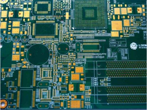
1. PCB wiring direction From the welding surface, the arrangement orientation of components should be consistent with the schematIC diagram as much as possible, and the wiring direction should be consistent with the wiring direction of the circuit diagram. Since it is usually necessary to detect various parameters on the welding surface during the production process, this is convenient for production
1. Wiring direction
From the welding surface, the arrangement orientation of PCB components should be consistent with the schematic diagram as much as possible, and the wiring direction should be consistent with the wiring direction of the circuit diagram. Since various parameters are usually required to be tested on the welding surface during the production process, this is convenient for inspection, debugging and maintenance in production (Note: it refers to the prEMIse of meeting the requirements of circuit performance and the layout of the installation panel of the whole machine).
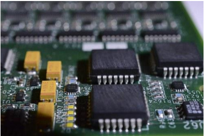
2. Arrangement of components
The distribution shall be reasonable and even, and the process requirements of neat, beautiful and rigorous structure shall be met.
3. Placement of resistance and diode
It is divided into horizontal and vertical placement:
(1) Horizontal placement: When the number of circuit components is SMAll and the size of the circuit board is large, it is generally better to use horizontal placement; When the resistance below 1/4W is placed horizontally, the distance between two pads is generally 4/10 inches, and when the resistance below 1/2W is placed horizontally, the distance between two pads is generally 5/10 inches; When the diode is laid horizontally, 1N400X series rectifier tube is generally 3/10 inch; 1N540X series rectifier tube, generally 4~5/10 inches.
(2) Vertical placement: When the number of circuit components is large and the size of the circuit board is small, vertical placement is generally adopted. The spacing between two pads is generally 1~2/10 inches.
4. Potentiometer: placement principle of PCB chip (IC) base
(1) Potentiometer: it is used to adjust the output voltage in the voltage regulator. Therefore, the design of the potentiometer should increase the output voltage when it is fully adjusted clockwise, and decrease the output voltage when it is adjusted counterclockwise; In the adjustable constant current charger, the potentiometer is used to adjust the charging current fold. When the potentiometer is designed to be full and adjusted clockwise, the current will increase.
The position of the potentiometer should meet the requirements of the whole machine structure installation and panel layout, so it should be placed at the edge of the board as far as possible, with the rotary handle facing outward.
(2) IC base: When designing the printed board drawing, when using the IC base, pay special attention to whether the positioning slot on the IC base is placed in the correct direction, and whether each IC pin position is correct. For example, the first pin can only be located at the lower right corner or upper left corner of the IC base, and close to the positioning slot (from the welding surface).
5. Arrangement of incoming and outgoing terminals
(1) The distance between the two associated lead ends should not be too large, generally about 2-3/10 inches.
(2) The incoming and outgoing line ends shall be concentrated on 1 to 2 sides as far as possible, and shall not be too discrete.
6. When designing the wiring diagram, pay attention to the order of pin arrangement, and the spacing between component pins should be reasonable.
7. On the premise of ensuring the circuit performance requirements, the design shall strive for reasonable wiring, less use of external jumper, and PCB wiring according to certain charging requirements, so as to be intuitive, convenient for installation, height and maintenance.
8. When designing the wiring diagram, the routing shall be as SIMple and clear as possible.
9. PCB layout line width and line spacing shall be moderate, and the spacing between two bonding pads of capacitor shall be consistent with the spacing between capacitor lead pins as far as possible;
10 PCB design shall be carried out in a certain order, such as from left to right and from top to bottom.


抖音二維碼

Q Q二維碼

微信二維碼
點擊
然后
聯系
然后
聯系
電話熱線
13410863085Q Q

微信

- 郵箱