鑫景福致力于滿足“快速服務,零缺陷,輔助研發”PCBA訂購單需求。


行業新聞
Selection and Welding of Solder Template for PCBA Processing components
In the whole schematIC drawing stage, PCBA factory considered the need of pattern decision in the layout stage to ensure that sufficient bypass capacitors and interface layers were designed SMT technology uses integrated circuits Make sure that appropriate decoupling capacitors are used near the ground (preferably at the ground level). The proper size of the capacitor depends on the application, the surface mounting technology of the capacitor mounting factory, and the frequency involved When the bypass capacitor is placed at both ends of the power and ground pins and close to the corresponding IC pin, the electromagnetic compatibility and magnetic sensitivity efficiency of the circuit will be optimized
The SMT technicians in the PCB factory (BOM) operate the bill of materials to check the virtual parts. These parts have no contour associated with them and are not transferred to the layout. They generate the BOM and view all the virtual components in the design. The only entries should be power and ground signals, PCBAa processing, because they are considered as virtual parts and are processed only in the schematic environment and not in the layout, unless they are only used for analogy purposes. The part displayed in the virtual part should be replaced with a part with a footprint.

Check whether there is enough data in the BOM report. After running the BOM report, check and continue to fill in any incomplete parts, supplier SMT patches or manufacturer information of all these parts.
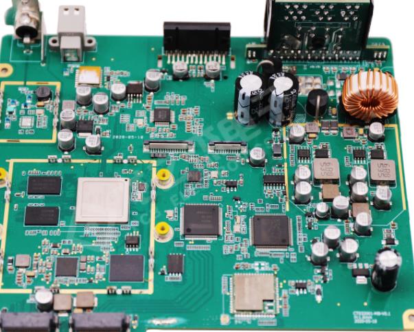
"SIMilar to other manufacturing technologies, in the SMT process of PCBA assembly, there are many factors that will affect the reliability and functionality of printed PCBA circuit boards. These factors include the information and design of the template used, the placement of solder paste, and various components. Considering the actual PCBA and SMT equipment used and the specific requirements required, we also analyzed them. In the process of PCB processing in the SMT chip processing plant, it is important to weld the template and solder Connect.
Welding template and repair welding.
In PCB processing of SMT board factory, the thickness of sample wire MESh usually matches the needs of all components in PCB. Solder paste can be applied to PCB through screen printing, and its volume is determined by the thickness and aperture of the template. If the thickness of the template does not match all components on the same plate, a reduced pressure template will be considered.
In the SMT chip assembly process of PCBA, SMR Technology uses electroforming templates made of nickel or stainless steel to ensure uniform and high-quality welding of plates. In addition, it is recommended to bypass the corners of the holes to provide good paste release. The hole of the solder joint must be the same size as the metal pad placed on the PCBA board. Finally, for best results during assembly, the template should be folded into SMAller openings.


抖音二維碼

Q Q二維碼

微信二維碼
點擊
然后
聯系
然后
聯系
電話熱線
13410863085Q Q

微信

- 郵箱