鑫景福致力于滿足“快速服務,零缺陷,輔助研發”PCBA訂購單需求。


行業新聞

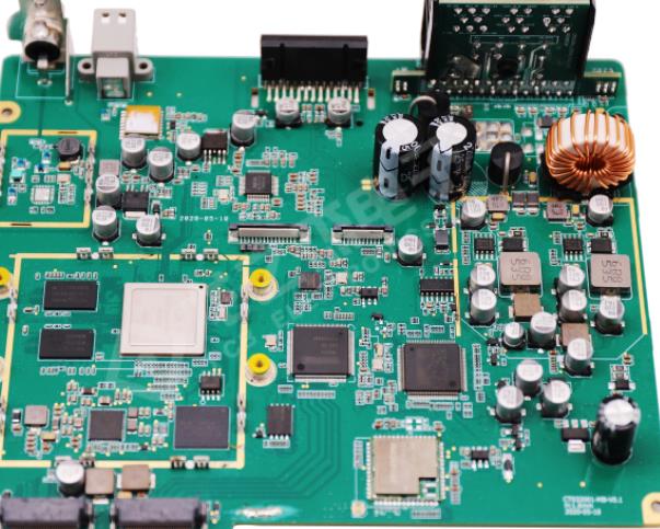
SMT process specifICation for PCBA manufacturing
Process requirements for installing components:
1. The model, model, nominal value and polarity of components at each assembly position shall be MARKed as meeting the requirements of assembly drawing and product list.
2. The instalLED components shall be intact.
3. When the thickness of the welding end or leg of the mounting element is not less than 1/2, the solder paste will be penetrated. It is used to extrude the solder paste when repairing general parts. The narrow gap assembly patch shall be less than 0.2mm and less than 0.1M.
4. The terminal or pin of the component is aligned and centered with the pattern of the pad. Due to the self positioning effect of PCB in the process of flow soldering, there may be some deviation in the installation position of components. The allowable deviation range is as follows
Rectangular component: PCB pad under correct design, the component width is greater than 3/4 of the width direction of the welding end on the adhesive pad. After the welding end of the component in the length direction overlaps with the adhesive pad, the protrusion of the adhesive pad is greater than 3/3 of the height of the welding end, and more than 3/4% of the width of the welding end of the component must be placed on the adhesive pad During installation, pay special attention to the contact between the welding end of the component and the solder paste
SMAll transistor SOT. X, Y, T rotation angles are allowed. There is deviation, but all pins must be on the PCB pad.
Small integrated circuit SOTC. X, Y, T rotation angles are allowed. There is an installation deviation, but it must be ensured that 3/4 of the component pin width is located on the PCB pad.
Quadrilateral flatpack assembly and subminiature package assembly QFP. To ensure that the pin width of 34 is located on the PCB pad, X, Y, T are allowed to have small installation deviation.

Correct components
The type, model, nominal value and polarity of components at each assembly position shall meet the requirements of assembly drawing and product list, and shall not be misaligned.
Polychlorinated biphenyls
positioning accuracy
1. The end or pin of the element shall be aligned and centered with the pattern of the pad as far as possible, and the welding of the element shall be in contact with the solder paste.
2. The placement of components must meet the process requirements.
The self positioning effect of the two chip modules is greater. During installation, the component width exceeding 12-3/4 is overlapped on the PCB pad. As long as both ends overlap on the corresponding PCB pad and touch the paste pattern, they can be automatically positioned during flow soldering. However, if one end does not overlap on the PCB pad or touch the paste pattern, displacement or suspension bridge will occur during reflow soldering.
The self positioning effect for SOP, SOJ, OFP, PLCC and other equipment is small, and reflow welding cannot correct the installation offset If the installation position exceeds the allowable deviation range, the SMT operator must dial manually before entering the reflow furnace Otherwise, repair is needed after reflow soldering, which will lead to excessive waste of working time and data in PCB factories, and even affect the reliability of product quality When it is found that the installation position exceeds the allowable range, the installation coordinate PCBA processing shall be corrected in time
Manual installation or manual dialing requires an accurate installation position. The pin is aligned with the pad and centered. If the placement is inaccurate, please drag and paste to find the right side. One side of the pasted figure is glued, causing bridging.
Pressure patch height. Appropriate tip pressure Z-axis height. Be appropriate.
The patch pressure is too low, the welding end or solder leg of the element is on the surface of the solder paste, the solder paste cannot adhere to the element, and the position is intentionally moved during transfer and reflow soldering. In addition, if the Z axis is too high, the component will fall from the height when patching, which will cause the patching position to shift.
Patch overpressure and excessive paste extrusion are easy to cause paste adhesion. Bridging is easy to occur during reflow soldering. At the same time, the position of the patch will shift due to sliding, which may damage the components in serious cases


抖音二維碼

Q Q二維碼

微信二維碼
點擊
然后
聯系
然后
聯系
電話熱線
13410863085Q Q

微信

- 郵箱