鑫景福致力于滿足“快速服務(wù),零缺陷,輔助研發(fā)”PCBA訂購單需求。


行業(yè)新聞
Causes and hazards of PCB component deformation
Causes of PCB assembly deformation
Deformation of CCL PCB manufacturer: Generally, the PCB manufacturer is a double-sided board with symmetrICal structure and no graphics The thermal expansion coefficients of copper foil and glass cloth are almost the same, so PCB manufacturers can hardly cause PCB board deformation due to their different thermal expansion coefficients However, due to the large size of the CCL press and the large temperature difference in different areas of the hot plate, the resin curing speed and degree in different areas are slightly different during the bonding process At the same time, the dynamic viscosity under different heating rates will also be very different. In addition, due to the differences in the curing process, local stress will also be generated Usually, this kind of pressure will be pressed together on PCB boards, but PCBA manufacturing will be gradually released in the subsequent process of PCB, resulting in PCB board distortion

PCB bonding of PCB manufacturers: PCB bonding process is the main process of generating thermal stress. It is SIMilar to the bonding of copper clad laminate, but it will also produce local stress due to the difference of curing process. Due to such factors as large thickness, diverse pattern distribution, and more sEMI cured plates, the thermal stress in the bonding process of PCB is more difficult to eliminate than that of CCL. The stress in PCB is released during drilling, forming or baking, which is also easy to cause PCB deformation.
The PCB is deformed through resistance welding and character baking: since the resistance inks cannot be stacked with each other during curing, the PCB will be vertically solidified in the rack. The resistance temperature is about 150 C, which is just above the Tg point of the medium and low Tg data. The resin above the Tg point has high elasticity. The PCB board is easy to deform under the action of its own weight or strong wind in the oven.
Hot air solder leveling deformation: the temperature of the hot air solder leveling tin furnace for ordinary pcb is 225 ~ 265 C, the time is 3S-6S, and the hot air temperature is 280 ~ 300 C. The solder leveling PCB enters the tin furnace from room temperature, and two minutes after the furnace is out, after treatment and cleaning at room temperature, the whole hot air solder leveling process is a process of sudden heating and cooling of PCB. Due to the uneven structure of PCB printed circuit board data, thermal stress will inevitably be generated during cooling and heating, resulting in micro strain and overall deformation of PCB.
Storage deformation: PCB assembly boards of PCB manufacturers are usually stuck on the shelf in the semi-finished product stage. During storage, improper adjustment of the tightness of shelf or PCB assembly board stack may cause mechanical deformation of PCB assembly board, especially for PCB assembly boards below 2.0 mm. In addition to the above factors, there are many other factors that affect the deformation of PCB assembly board.
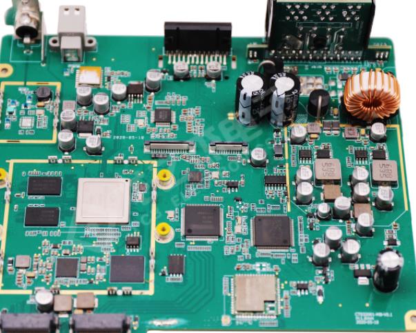
Causes and hazards of PCB assembly
Hazards of PCB assembly deformation
If the PCB board is not flat, the surface mounting line of the PCB automatic placement machine will lead to improper positioning. This PCB component cannot be instalLED or installed on the board of directors of the PCB component and the surface mounting pad of the PCB component. Even the automatic plugger of the PCB component will be damaged
After the PCB assembly is welded, the components are bent, the PCB assembly at the bottom of the assembly is difficult to cut flat, and the PCB assembly cannot be installed on the machine's main housing or socket Therefore, PCB assembly factories also have trouble with PCBA board warping when encountering problems At present, SMT technology is developing towards high precision and high speed intelligence This requires circuit board components as various components to have higher smoothness IPC standard clearly points out that the surface mounting equipment of PCB components is 0.75% and the s of PCB boards without surface mounting is 1.5%
In fact, in order to meet the requirements of high-precision and high-speed SMT installation, some electronic installation PCB component manufacturers have stricter requirements on deformation, such as 0. 5%, or even 0.3% personal requirements
PCB board is made of copper foil, resin, glass cloth and other materials. Each material has different physical and chemical properties. When pressed together, thermal stress will remain, resulting in PCB deformation and warping.
At the same time, PCB manufacturing technology will go through various processes, such as high temperature, mechanical cutting, wet processing, and will also have an important impact on the deformation of PCB components In a word, the causes of PCB deformation may be complex and diverse. How to reduce or eliminate PCB component manufacturing based on different data characteristics It has become one of the complex problems we are facing
It is necessary to study the deformation of PCB components in terms of data, structure, graphic distribution, PCB manufacturing technology, etc. The uneven area of copper laying on PCB will worsen the bending and warping of PCB.
Generally, a large area of copper foil is designed on the PCB for grounding. SometiMES there is a large area of copper foil in the Vcc layer. When these large areas of copper foil are unevenly distributed on the same PCB, it will lead to uneven heat absorption and heat dissipation. PCB printed circuit board will definitely expand and shrink. If the expansion and contraction cannot cause different stresses at the same time, the PCB assembly will be deformed. At this time, if the temperature of the circuit board has reached the upper limit of Tg value, the PCB will begin to soften, causing PCB deformation. The connection points (via) of each layer on the PCB will limit the expansion and contraction of the PCB.
Today's PCB boards are mainly multilayer PCB boards, and this re will be driven like connection points (vias) between this layer, which is divided into through holes, blind holes and buried holes Where there are connections, the expansion and cooling effect of the PCB assembly will be limited, and the PCB will be indirectly twisted in the following cases: the PCB assembly has been used


抖音二維碼

Q Q二維碼

微信二維碼
點擊
然后
聯(lián)系
然后
聯(lián)系
電話熱線
13410863085Q Q

微信

- 郵箱