鑫景福致力于滿足“快速服務,零缺陷,輔助研發(fā)”PCBA訂購單需求。


行業(yè)新聞

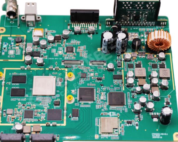
Introduction to the process from bare PCB to PCBA
From bare PCB to PCBA, let a ?? s explain in detail below:
1. SMT placement process
SMT (Surface Mounted Technology) is a Surface Mount Technology (surface mounted Technology), whICh is one of the most popular technologies and processes in the electronic assembly industry
To put it SIMply, it is a kind of surface mount components without leads or short leads (SMC/SMD abbreviation, chip components in Chinese) mounted on the surface of a Printed Circuit Board (PCB) or the surface of other substrates Above, a circuit assembly technology that is assembLED by welding, reflow or DIP welding
Polychlorinated biphenyls

So, what preparations should be made before surface mounting?
1). PCB must have a MARKing point, also known as reference point, which is common for the placement of the placement machine and is equivalent to a reference object;
2). Transfer the exact amount of solder paste to the exact position on the empty PCB;
3). SMD programming: According to the BOM provided, the components are accurately positioned and placed in the corresponding positions of PCB through programming
After all the above preparations are completed, SMT mounting can be carried out
First, the mounter determines whether the circuit board is in the correct direction according to the marked points on the circuit board sent to it, and then brushes the solder paste on the mold, and the solder paste is deposited on the PCB pad through the template
Next, the placement machine will place the components in the corresponding positions of PCB according to the placement program design, and then conduct reflow soldering to effectively contact the components, solder paste and circuit board
Finally, an automatic optical inspection is performed to check the components on the PCB board, where: virtual welding, solder connection, device orientation, etc, However, since there are soldered pieces on the circuit board, the function inspection cannot be performed
It should be noted that some devices have positive and negative poles or pin sequences. Therefore, it is necessary to check the incoming materials to prevent the repair of errors, especially BGA packaging devices If the direction is wrong, subsequent disassembly and repair welding are time-consuming and laborious
2. The DIP plug-in process
DIP (dual in line package) is English abbreviation for dual in line package In fact, it is a kind of equipment that can perforate and weld on PCB board, usually called "component assembly"
What preparation should be made before DIP?
1). Prepare the furnace fixture and fix the PCB board to facilitate the transmission on the conveyor belt;
2). Need to correct the pins of plug-in devices with too long pins to a proper length;
3). It requires manpower to insert the plug-in device into the through hole of the corresponding PCB
Next, briefly describe the DIP assembly process: The DIP assembly process is much simpler than the SMT mounting process, but inserting the plug-in components into the corresponding holes requires manual assistance, and then through the wave soldering machine, the DIP assembly is perfectly welded to the PCB
Some people may worry that the solder in the welding pool is not splashed on the entire circuit board?
The answer is no The solder in the solder pool will only adhere to the place where it contacts the metal, and will not adhere to the green solder mask This is the role of solder mask
After welding plug-in equipment, is the PCB complete? Of course not, because the circuit board after wiring and components has also been checked and verified
3. Carry out functional test on the products produced. Polychlorinated biphenyls
PCBs can be divided into two steps:
The first step: human visual inspection of polychlorinated biphenyls, preliminary screening of defective boards, such as tin connection, false welding, welding and other visible errors can not be seen by the naked eye, and then send defective circuit boards for repair. The circuit boards without problems will enter the second step
Step 2: Check PCBs using a test fixture, which is actually PCBs Use the test fixture to test PCBs, such as: power on and power off, relay pickup, expression, etc, Determine whether each SMAll module on the board works normally
After the above two screening steps, not only the problem boards can be screened, but also the problems of the problem boards can be determined during the screening process, which reduces the workload of subsequent maintenance of the fault boards
Therefore, it can be seen that scientific and technical personnel have carried out strict and comprehensive tests on every step from bare PCB to PCBs, just to ensure that every step in the production process is normal Only in this way can we continue step.
4. Water tight, dust-proof and anti-corrosion polychlorinated biphenyls
Waterproof, dustproof and anti-corrosion treatment is to spray or dip wax on PCBs Each company may have its own treatment pipeline. Some people apply 3 anti paint manually, some machines spray 3 anti paint, and some are dipped in wax. Of course, some people do not do treatment
At this point, from bare PCB to PCBA are introduced


抖音二維碼

Q Q二維碼

微信二維碼
點擊
然后
聯(lián)系
然后
聯(lián)系
電話熱線
13410863085Q Q

微信

- 郵箱