鑫景福致力于滿足“快速服務(wù),零缺陷,輔助研發(fā)”PCBA訂購單需求。


行業(yè)新聞
Protection of PCBA proofreading chip assembly
With the development of electronIC product technology, circuits are becoming more and more intensive, the number of components on a single board is increasing, and the risk of component damage is also increasing In this paper, how to calibrate and place PCBs to avoid damage is described in detail
Operational issues leading to collisions
Process damage Impact fracture, stress damage
1 Improper casing setting
When bending stress is applied to the component or the test is conducted, the adjacent support will be damaged.
The damage of resistor is characterized by breakage or electrode peeling, and the capacitor is in inclined crack mode. If it is the first process part, the tombstone of broken parts may appear after reflow.
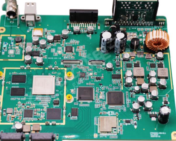
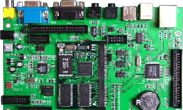
How to protect many PCB proofing chip elements
Circuit board

2 Stress damage
Poor plate feeding results in deformation or manual bending of the clamping plate (clamping plate); Poor suction nozzle and improper height setting may damage components.
The typical feature of PCBs proofing patch damage is frontal cracking, and the fracture is usually separated after passing through the furnace; If the side is damaged, most of the slope will be cut off In this case, the location of the impact point can be clearly distinguished
Operational issues leading to collisions
Damage after process impact fracture,
Stress damage, delamination (thermal shock)
1 Impact fracture
In the lateral impact, it is usually not easy to judge the impact point of the polychlorinated biphenyl anti-static patch, because the patch usually peels off (resistance) or the part electrode breaks (capacitance); The longitudinal collision part is easier to identify the collision point, and the pad is usually not damaged, but you can see the corner where the part is obviously missing.
2 Stress damage
Damage caused by pressure and bending caused by folding of plate edges, test fixture, trolley placement, etc. This type of damage usually occurs in the form of diagonal cracks.
3-layer stripping
It is caused by improper welding repair. Typical features are burnt black flux near the part, rough surface discoloration, layer peeling (capacitance), character surface peeling, etc.
How to start analyzing damaged parts
1 Analysis points according to impact
The existence of the impact point is not an absolute analysis and judgment factor, but usually the location, direction and damage degree of the impact point will provide a lot of analysis information.
a. The linear impact force usually damages the PCB, and obvious damage defects can be seen on the components.
b. The parallel impact force will directly cause damage to parts due to cracks and missing angles, but due to the SMAll torque direction, it will not cause serious damage to the gasket in most cases.
2 According to crack shape
a. Delamination crack: most of the delamination is caused by thermal shock, but part of the reason is poor component manufacturing, because interlayer bonding and baking process defects lead to delamination after reflow welding.
b. Inclined crack: the bending stress forms a fulcrum at the lower part of the part, and the fixed solder joint produces a crack inclination at the electrode end, especially the large components perpendicular to the stress direction are most seriously fractured.
c. Radial cracks: radial cracks usually have the following impact points, which are mainly caused by point pressure, such as casing, suction nozzle, test fixture, etc.
d. Complete fracture: Complete fracture is the most serious failure mode, which is often accompanied by PCB damage It is usually caused by lateral impact or capacitor crack, resulting in equipment burning
3 According to the displacement of parts
When the PCB proofing patch parts have longitudinal cracks or reflow heating but are not cracked, it is likely that only cracks will be seen but not separated, which will lead to inspection problems. Due to the tension of solder melting, the cracks generated before reflow will be pulLED away. Even during reflow, there will be a tombstone at the broken part. Most of the reasons are component damage in the first process, bending stress or improper ejector pin setting in the second process. Of course, cracks caused by cutting and packaging during component manufacturing may also be cracked due to the heat after reflow welding.
The above is the explanation given by the editor of pcb circuit board company.
If you want to know more about PCBA, you can go to our company's home page to learn about it.
In addition, our company also sells various circuit boards,
High Frequency Circuit Board and SMT chip are waiting for your presence again.


抖音二維碼

Q Q二維碼

微信二維碼
點(diǎn)擊
然后
聯(lián)系
然后
聯(lián)系
電話熱線
13410863085Q Q

微信

- 郵箱