鑫景福致力于滿足“快速服務,零缺陷,輔助研發”PCBA訂購單需求。


行業新聞
design of Functional PCB Based on RF Switch Module
Modern wireless communICation system, mobile communication, radar, satellite communication and other communication systems with printed circuit board have higher requirements for switching speed, power capacity, integration, etc VXI bus module is of great significance to the special requirements of the Party We will use the idea of virtual instrument to realize the hardware circuit in the form of software The RF switch designed below can be directly controlLED by a computer and can be easily connected to the VXI bus test system It has broad development prOSPects to integrate and maximize the application of computer and microelectronics technology in today's testing field
Circuit board

1. Design and implementation of VXI bus interface circuit
VXIbus is an extension of VMEbus in this field of instrumentation and is a computer operated modular automatic instrumentation system It relies on effective standardization and adopts modular method to realize serialization, generalization, interchangeability and interoperability of VXI bus bar instruments Its open architecture and Plug&Play method fully meet the requirements of information products. It has the advantages of high-speed data transmission, compact structure, flexible configuration, good electromagnetic compatibility, etc, This system is very convenient to set up and use. It has been used more and more widely, and has gradually become an integrated bus of high-performance test system
VXI bus bar is completely open and applicable to modular instrument backplane bus bar specifications of various instrument manufacturers VXI bus devices are mainly divided into register based devices, MESsage based devices and memory based devices The current promotion of register based devices in applications (about 70%) The interface circuit based on VXI bus register mainly includes four parts: bus buffer drive, addressing and decoding circuit, data transmission response state machine, configuration and operation register set In the four parts, bus buffer driver is implemented by 74ALS245 chip, and the rest is implemented by FPGA FLEX10K chip EPF10K10QC208-3 and EPROM chip EPC1441P8 are used, using the responding software MAX+PLUS2 to design and implement
1.1 Bus buffer driver
This part completes the buffer receiving or driving of the data line, the address line and control line in the VXI backplane bus bar, to meet the requirements of VXI standard signals For A16/D16 devices, only buffer drive of backplane data buses D00 ~ D15 is realized According to the requirements of VXI bus specification, this part is implemented by two 74LS245s, and is added with DBEN * (generated by the data transmission response state machine)
1.2 Addressing and Decoding Circuits
The addressing lines include address lines A01-A31, data strobe DS1 * 0 * * and DS1 *, and long text line LWORD * * The control lines include address spoke lines AS * and read/write signal lines The design of this circuit adopts the schematIC design method of MAX+PLUS II. The existing components in the assembly library are used for design. Two 74688 and one 74138 are used. The function module decodes the address line A15-A01 and the address modification line AM5-AM0. When the device is addressing, it receives the address information on the address line and the address modification line, and compares it with the logical addresses LA7~LA0 set by the hardware address switch on the module If the logical value on AM5~AM0 is 29H or 2DH (Because it is an A16/D16 device), when the address lines A15 and A14 are both 1, the logical value on A13-A06 is equal to the logical address of the module, and the device is addressed and spoke (CADDR * is true) Then send the result to the lower decoding control, and select the register of the module in the 16 bit address space through the decoding address A01-A05
1.3 Data transmission response state machine
Data transmission bus is a group of high speed asynchronous parallel data transmission bus, which is the main component of VMEbus system information exchange The signal lines of the data transmission bus can be divided into three groups: address lines, data lines, and control lines The design of this part adopts the text input design method of MAX+PLUS2. Since the timing of DTACK * is more complicated, it is designed and implemented by state machine using AHDL language This functional module includes control signals in the VXI backplane bus, and provides timing and control signals for the standard data transmission cycle (generating the data transmission enable signal DBEN *, the bus response signal DTACK * required for data transmission, etc.) During data transmission, the system controller first addresses the module and sets the corresponding address strobe lines as * *, data strobe lines DS0 *, DS1 *, and WRITE * signal lines that control the direction of data transmission to valid level It drives DTACK * to a low level to confirm to the bus controller that the data has been placed on the data bus (read cycle) or that data has been successfully received (write cycle)
1.4 Configuration Register
Each VXI bus device has a set of "configuration registers". The main controller of the system obtains some basic configuration information of VXI bus devices by reading the contents of these registers, such as device type, model, manufacturer, address space (A16, A24, A32) and the required storage space The basic configuration registers of VXI bus bar devices are: identification register, device type register, status register, and control register The design of this part of the circuit adapters the schematic diagram design method of MAX+PLUS II, and use 74541 chip, a functional module created by it The ID, DT, and ST registers are read-only, and the control register is a write only register In this design, VXI bus bars are mainly used to control the on-off of these switches Therefore, as long as the data is written to the channel register, the ON/OFF status of the relay switch can be controlled The inquiry relay status is also read from the channel register data. According to the design requirements of the module, write appropriate content in each corresponding data bit to effectively control the RF switch of the functional module
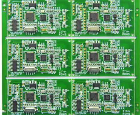
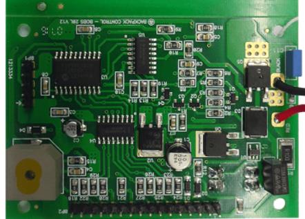
2. PCB board for module functional circuit design
Each VXI bus device has a set of "configuration registers". The system master controller obtains some basic configuration information of VXI bus devices by reading the contents of these registers, such as device type, model, manufacturer, address space (A16, A24, A32) and the required storage space The frequency range of RF circuit is about 10kHz to 300GHz With the increase of frequency, RF circuit has some characteristics different from low frequency circuit and DC circuit Therefore, when designing the RF circuit of PCB board, it is necessary to pay special attention to the RF signal on PCB board The RF switch circuit is controlled by VXI bus bar In order to reduce the interference in the design, the cable is used to connect the bus interface circuit and the RF switch function circuit The following mainly introduces the RF switch function circuit of PCB board
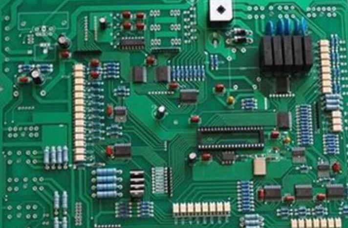
2.1 Layout of components
Electromagnetic compatibility (EMC) refers to the ability of an electronic system to function
normally in a specified electromagnetic environment as designed. For RF Circuit PCB design, electromagnetic compatibility requires that each circuit module should not generate electromagnetic radiation as far as possible, and have certain anti electromagnetic interference capability The layout of components directly affects the interference and anti-interference capability of the circuit itself It also directly affects the efficiency of the designed circuit
General principle of layout: components should be arranged along the same direction as far as possible. By selecting the direction of PCB entering the tin melting system, bad soldering can be reduced or even avoided; The spacing between components must be at least 0.5mm to meet the requirements for tin melting of components. If the PCB allows, the spacing between components should be as wide as possible Reasonable layout of components is also a prerequisite for reasonable wiring, so it should be considered comprehensively In this design, the relay is used as a channel for converting RF signals. In summary, the relay should be as close to the signal input and output as possible, so as to shorten the length of RF signal line as possible, and make reasonable wiring for the next step Consider In addition, RF switch circuit is controlled by VXI bus, and the influence of RF signal on VXI bus control signal must be considered in layout
The above is the explanation given by the editor of pcb circuit board company.
If you want to know more about PCBA, you can go to our company's home page to learn about it.
In addition, our company also sells various circuit boards,
High Frequency Circuit Board and SMT chip are waiting for your presence again.


抖音二維碼

Q Q二維碼

微信二維碼
點擊
然后
聯系
然后
聯系
電話熱線
13410863085Q Q

微信

- 郵箱