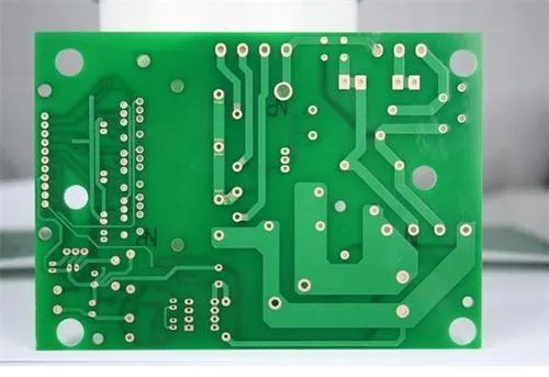

The design Process of SMT smt pcb
What is the purpose of the design process
1. Design power schematIC diagram
The main work of electric power schematIC design is to use software to draw circuit schematic diagram and compile to generate network table.
What is the design process of SMT SMT PCB
2. Create PCB file
By creating PCB files, the PCB editor is calLED and the design is completed in the PCB editing environment
What is the design process of SMT SMT PCB

3. Planning circuit board
Before drawing the printed circuit board, the designer should also plan the circuit board, including defining the size and shape of the circuit board, setting the layers of the circuit board and setting parameters. This is an extremely important task and the basic framework of circuit board design.
What is the design process of SMT SMT PCB
Circuit board
4. Load component package library and netlist
To place a component on a PCB, you need to load the package library of the component you are using first. Otherwise, when you import schematic information into a PCB, you cannot call the component package, resulting in errors.
What is the design process of SMT SMT PCB
5. Layout of components
Layout is to place components in proper positions on the printed board. Here, "appropriate position" has two meanings. First, the position of components can make the whole circuit board meet the requirements of electrical signal flow design and anti-interference, and look clean and beautiful; The other is that the location of components is favorable for wiring.
What is the design process of SMT SMT PCB
6. Set wiring rules
For components and network labels with special requirements, it is usually necessary to set routing rules before routing, such as safe spacing, line width, routing layer, etc.
What is the design process of SMT SMT PCB
7. Wiring
Wiring is the laying of copper wires to realize the electrical connection between various pads. This can be done automatically or manually. The automatic routing function of Altium Designer 10 is very powerful. If the component layout is reasonable and the routing rules are set correctly, the success rate of automatic routing is close to 100%; If automatic routing cannot be completely resolved or routing conflicts occur, you can adjust them through manual routing.
What is the design process for? SMT patch printed circuit board
8. Generate report and print
After the circuit board wiring is completed, save the PCB diagram, and then use various graphic output devices to output the PCB diagram. After the PCB diagram is designed according to the above process, the files can be handed over to the PCB production unit for production.
The above is about the design process of SMT chip printed circuit board, and I hope it can help you.
然后
聯系
電話熱線
13410863085Q Q

微信

- 郵箱


