鑫景福致力于滿足“快速服務(wù),零缺陷,輔助研發(fā)”PCBA訂購單需求。


行業(yè)新聞

production process of SMT patch processing template
Requirements for SMT chip processing template production process
1. What are MARK's processing steps?
1. Mark processing method, whether it is necessary to mark, and place it on the side of the template.
2. The side on whICh the marking pattern is placed shall be determined according to the specific structure of the printing machine (the position of the CAMera).
3. The engraving method of the mark points depends on the printing machine, including printing surface, non printing surface, half engraving on both sides, full engraving and seaLED vinyl, etc.
2. Whether to join the board of Directors and the requirements of the Board of Directors. If the circuit board is assembled, the PCB file of the circuit board shall be given.
Third, it is required to insert the backing ring. Since plug-in components use reflow soldering process, this requires more solder paste than installation components. If plug-in components need reflow soldering process, special requirements can be put forward.
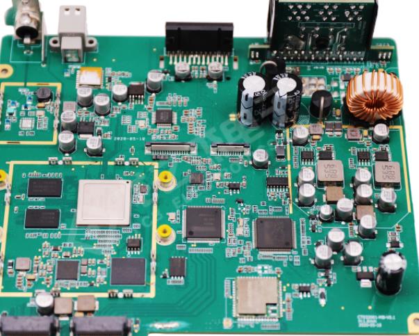
Circuit board
Fourth, the modification requirements for the size and shape of the model (pad) opening. For pads generally larger than 3mm, in order to prevent the solder paste pattern from sinking and prevent solder beads, the opening adopts the "bridging" method. The line width is 0.4mm, and the opening is less than 3mm, which can be divided equally according to the size of the pad. Various components have requirements for template thickness and opening size.
1. The print quality of mBGA/CSP with square opening and flip chip is better than that of circular opening.
2. When the cleaning solder paste is not used and the cleaning process is not used, the opening size of the template should be reduced by 5% - 10%:
3. The opening design of lead-free process template is larger than that of lead, and solder paste should cover the bonding pad as much as possible.
4. The proper shape of the opening can improve the processing effect of the patch. For example, when the size of the wafer component is SMAller than metric 1005, because the distance between the two pads is very small, the solder paste on the pads at both ends of the wafer is easy to adhere to the bottom of the component, and it is easy to generate the bottom of the component after reflow soldering. Bridge and welding ball. Recall that when handling the template, the interior of a pair of rectangular pad openings can be modified to sharp or bow shape to reduce the amount of solder paste at the bottom of the part, which can improve the welding sound adhesion at the bottom of the part during placement, as shown in the figure. The specific modification scheme can be determined by referring to the "Design of the opening of the printing solder paste template" of the template processing factory.
5、 Other requirements
1. According to PCB design requirements, whether the test point needs to be opened, etc, If the test point is not specified, it will not be opened
2. Whether there are requirements for electropolishing process. The electrolytic polishing process is used for samples with the opening center distance less than 0.5mm.
3. Purpose (specify whether the processed template is used for printing solder paste or printing paster).
4. Whether it is necessary to engrave text on the template (PCB product code, template thickness, processing date and other information can be engraved, but cannot be passed).
6. After receiving Email and fax, the sample processing factory will send back the fax "Ask the Buyer for confirmation" according to the requirements of the Buyer.
1. If you have any questions, please call or fax again and deal with them after the buyer confirms.
2. Check whether the size of the screen frame meets the requirements, place the template on the desk, press the stainless steel screen surface with your hand, and check the tension.
The higher the screen quality, the tighter the stretching, and the better the printing quality. In addition, check the bonding quality around the screen frame.
3. Lift the template for visual inspection, check the appearance quality of the template opening, and check whether there are obvious defects, such as the opening shape, the distance between adjacent openings of IC pins, etc.
4. Use a magnifying glass or microscope to check whether the horn of the pad opening is downward, whether the inner wall around the opening is smooth, and whether there are burrs. Focus on the processing quality of narrow pitch IC pin openings.
5. Place the printed board of the product under the template, align the leakage of the template with the grounding pattern of the printed board, and check whether the pattern is completely aligned, whether there are holes (unnecessary openings) and a few holes (floor drain openings).
6. If a problem is found, first check whether it belongs to our confirmation error, and then check whether there is a problem in processing If quality problems are found, PCB manufacturing shall be reported to the template and solved through negotiation


抖音二維碼

Q Q二維碼

微信二維碼
點(diǎn)擊
然后
聯(lián)系
然后
聯(lián)系
電話熱線
13410863085Q Q

微信

- 郵箱