鑫景福致力于滿足“快速服務,零缺陷,輔助研發”PCBA訂購單需求。


行業新聞
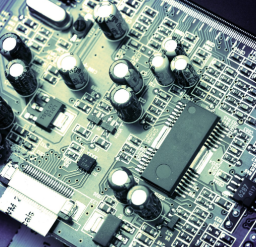
PCB vacuum etching technology
With the demand upgrading and rapid expansion of the global electronIC product MARKet, the miniaturization, high-precision, ultra-fine printed circuit board technology of electronic products is entering a rapid development period. In order to meet the increasing demand of the market, especially in the field of ultra-fine circuit technology, traditional and backward etching technology is being replaced by advanced vacuum etching technology. As a first-line PCB manufacturer, Honglian Circuit will show you the details of this technology
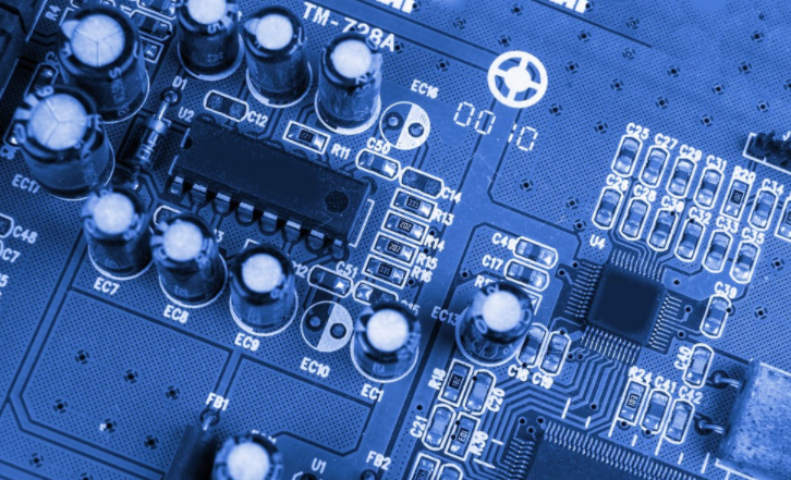
multilayer PCB

As we all know, it is not necessary to cover the surface of copper clad foil in all places. In order to produce circuit patterns, circuit board manufacturers will use chEMIcal solution etching to remove unwanted copper conductors, leave copper conductors, and form circuit patterns through subtractive process, which is calLED etching. It is the mainstream of current PCB processing.
The key to etching is the etching solution, the operating conditions of Circuit board manufacturers and the etching equipment. At present, acid copper chloride etching solution of copper chloride and hydrochloric acid and alkaline copper chloride etching solution of copper chloride and ammonia are the mainstream in the market. The PCB manufacturer controls the process parameters such as temperature, pressure, time and solution concentration to make the etching process in the best state. Etching equipment needs to be improved around production efficiency, etching speed and etching uniformity. At present, the main stream is horizontal transmission spray type.
Germany PILL e.K. released a new process technology, which can improve the fluidity of the etching solution on the board by absorbing the used etching solution, thus preventing the "pool effect". This method is called vacuum etching.
This method is confirmed by etching uniformity test with 35 μ The foil clad laminate of m copper foil is etched on both conventional and vacuum etchers, and the copper foil in the middle of the plate is etched to 18 μ Stop when the thickness is m, and detect the copper thickness distribution on the whole board surface. The thickness distribution of copper obtained by conventional etching of PCB batch manufacturers is usually high mountain in the center, while the thickness distribution of copper obtained by vacuum etching is uniform. Within the length of 600mm, the thickness difference between the center and the edge of conventional etching is about ± 4 μ m (18~10 μ m) While the thickness difference between the center and the edge of the vacuum etched copper is only about ± 1 μ m (19~17 μ m) The latter is only a quarter of the former.
The circuit board manufacturer adopts vacuum etching machine to make the line width/line spacing ≤ 30/30 μ M is easy to realize. In order to get the ideal effect, it is necessary to grasp the factors such as vacuum strength, spray pressure and copper foil thickness. The suction amount of the vacuum nozzle in the etcher to the plate solution should be equal to or slightly greater than the spray amount. If the suction amount is SMAll, the old solution will be detained. The spray pressure will affect the etching speed and the degree of side corrosion, but the pressure will damage the anti etching film, especially the distance between the details and the line pattern. For line width/line spacing=30/30 μ M line, the thickness of etched copper foil under conventional equipment is less than 12 μ m. Copper foil thickness during vacuum etching 18 μ M can also be processed. Reference data, line width/line spacing=30/30 μ m. Adoption 18 μ M copper foil, the suction capacity is 40Hz (about 120L/min) when the spray pressure is 0.1Mpa (1.02kgf/cm2), and the uniform line pattern is obtained.
This is the effect of vacuum etching technology. We can see that compared with traditional etching, vacuum etching is easier to control and more helpful to production efficiency.
The above is the explanation given by the editor of PCB circuit board company. If you want to know more about PCBA, you can go to our company's home page to learn about it. In addition, our company also sells various circuit boards,
High Frequency Circuit Board and SMT chip are waiting for your presence again.
How to distinguish the layers of PCB
10-24,2022


抖音二維碼

Q Q二維碼

微信二維碼
點擊
然后
聯系
然后
聯系
電話熱線
13410863085Q Q

微信

- 郵箱