鑫景福致力于滿足“快速服務(wù),零缺陷,輔助研發(fā)”PCBA訂購單需求。


行業(yè)新聞
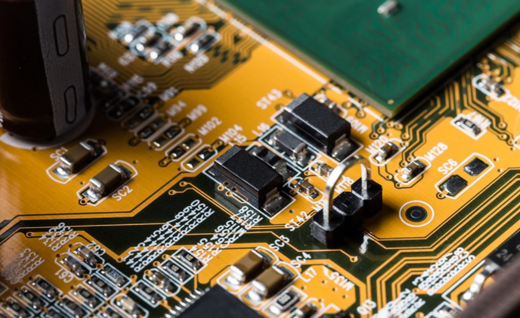
PCB proofing manufacturer: How do you see the layers of PCB?
First, visual inspection. Because the layers in PCB are closely combined, it is not easy to see the actual number. However, if you carefully observe the fault of the board, you can still distinguish it. Careful, we will find that there is a layer or several layers of white material sandwIChed between PCBs. In fact, this is the insulation layer between layers to ensure that there is no short circuit between different PCB layers. Because more single or double sided wiring boards are used in current multi-layer PCB boards, and a layer of insulation layer is placed between each layer of boards and then pressed, the number of layers of PCB board represents several independent wiring layers, and the insulation layer between layers becoMES the most intuitive way for us to judge the number of layers of PCB.
Second, guide hole and blind hole alignment method. The guide hole alignment method uses the "guide hole" on the PCB to identify the number of PCB layers. Its principle is mainly because the circuit connection of multilayer PCB adopts the pilot hole technology. If we want to see how many layers the PCB has, we can identify them by observing the guide hole.
On the most basic PCB (single sided motherboard), parts are concentrated on one side, and wires are concentrated on the other side. If you want to use a Multilayer board, you need to punch holes in the board, so that the component pins can pass through the board to the other side, so the guide holes will pierce the pcb board. Therefore, we can see that the pin of the part is welded on the other side.
For example, if the board uses four layers of boards, it is necessary to route in the first and fourth layers (signal layer). The other layers have other uses (ground wire layer and power layer). The purpose of placing the signal layer on both sides of the power layer and ground layer is to prevent mutual interference and to correct the signal line. If some board card pilot holes appear on the front side of the PCB, but cannot be found on the back side, it must be a 6/8 layer board. If the same pilot holes can be found on both the front and back of a PCB, it is naturally a 4-layer board.
However, at present, many board manufacturers use another routing method, that is, only some of the lines are connected, and the buried hole and blind hole technologies are used in routing. Blind hole refers to connecting several layers of internal PCBs with surface PCBs without penetrating the whole circuit board.
The embedded hole is only connected to the internal PCB, so it cannot be seen from the surface. Since the blind hole does not need to run through the entire PCB, if it is six layers or more, look at the board against the light source, and the light will not pass through. So there was also a very popular saying before: judge four and six or more layers of PCBs by whether the vias leak light. This method is reasonable, but also has some inapplicable points, which can be used as a reference method.

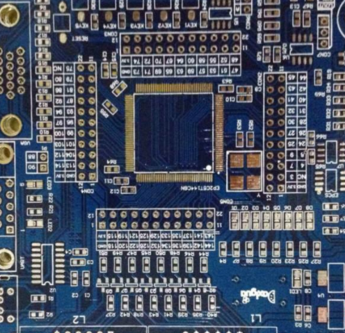
Third, the accumulation method. To be exact, this is not a method, but an experience. But this is what we think is the most accurate. We can judge the number of layers of a PCB by routing some male PCB cards and positioning components. Because in the current IT hardware industry, which is updating so fast, there are not many manufacturers who can redesign PCB.
For example, a few years ago, the 9550 graphics card with a large number of 6-layer PCBs was designed. Careful friends can compare it with the board type of 9600PRO or 9600XT? Only some components are omitted, and the height is consistent on the PCB.
In the 1990s, there was a widespread saying that the number of PCB layers could be seen by placing the PCB vertically, which many people believed. This statement was proved to be nonsense later. Even if the manufacturing technology at that time was still backward, how could the eyes tell the distance SMAller than the hair?
Later, this method continued and modified, and gradually evolved into another measurement method. Now many people believe that the number of PCB layers can be measured with precision measuring instruments such as "vernier caliper", which we also disagree with.
And no matter whether there is a precise instrument, how can we not see that the 12 layer PCB is three times thicker than the 4 layer PCB? Different PCBs will adopt different manufacturing processes, and there is no uniform standard to measure them. How to judge the number of layers according to the thickness?


抖音二維碼

Q Q二維碼

微信二維碼
點擊
然后
聯(lián)系
然后
聯(lián)系
電話熱線
13410863085Q Q

微信

- 郵箱