鑫景福致力于滿足“快速服務,零缺陷,輔助研發”PCBA訂購單需求。


行業新聞
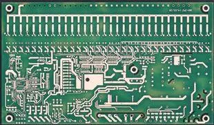
1、 SMT chip solder paste process
1. The tin spraying position printed on the PCB is centered with the bonding pad, and there is no offset of the ming display, whICh cannot affect the pasting and tin effect of SMT components.
2. The amount of tin sprayed on the PCB is moderate, and the pad cannot be completely covered, with less tin and missing brush.
3. The printing tin spraying point on the PCB is poorly formed. The printing tin spraying is connected with tin, and the tin spraying is concave and uneven. The tin spraying displacement exceeds one third of the bonding pad.
2、 SMT patch red glue process
1. The position of the red printing glue is in the middle, and there is no deviation of the ming display, which can not affect the pasting and soldering
2. The amount of red printing glue is moderate, which can be pasted well without insufficient glue.
3. The red glue dot of printing is offset between two pads, which may cause difficulty in tinning components and pads.
4. The amount of red glue is too much, and the width of the glue oozing from the lower side of the element body is more than half of the width of the element body.
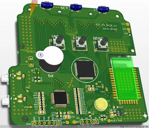
3、 SMT mounting process
1. SMT components shall be instalLED in order, in the middle, without deviation and skew.
2. The model and specification of SMT components at the mounting position should be correct, and the components should be reversed. The components are pasted reversely (it is not allowed to interchange the positions of two opposite sides of the components with differences, such as the upside down side of the side with silk screen MARK and the side without silk screen mark), so the function cannot be realized.
3. The mounting of SMD components with polarity requirements shall be processed according to the correct polarity marks. The device polarity is pasted reversely and wrongly (diode, triode, tantalum capacitor).
4. Soldering pads of multi pin devices or adjacent components shall be free of tin connection and bridging short circuit.
5. Solder pads of multi pin devices or adjacent components shall be free of residual solder beads and dross.
Future development of SMT chip processing
It is reported that today's mainstream mobile phone chips and some midrange chips use a brand's second generation 14nm process or TSMC's 16nm process. Maybe friends will think that today's process is still very advanced. But it actually seems to be out of date. As the 14nm process will become mainstream in 2017, the latest flagship processor released by a brand yesterday adopted the latest 10nm process. TSMC's 10nm process has begun mass production. As you can imagine, the size of current components is increasingly facing the limit. PCB design, the processing difficulty of SMT chips and the precision of automatic printing machine and placement machine have also reached the limit. The existing SMT mounting technology in the chip processing industry is difficult to meet the requirements of lighter and thinner portable electronic products and endless multi-function and high-performance.
Therefore, combining SMT chip solution technology with PCB production and manufacturing technology, a variety of new packaged composite components have emerged. In addition, in the production of multilayer boards, not only can passive components, such as resistors, capacitors, inductance coils, and ESD components, be produced internally, but also can be placed close to the pins of integrated circuit chips when needed, and some active components can be placed internally. The printed circuit board can not only be made SMAll, thin, light, fast and cheap, but also have better performance. In short, with the development of high-density packaging for small metal laser cutting machines, the boundary between primary packaging and secondary packaging becoMES more blurred. With the emergence of new components, there are also some new technology applications, which greatly promote the improvement of surface assembly technology Innovation and development make SMT processing technology more reliable in the more advanced and medium.
Today, I'd like to share it with you for the time being. For more information, please lock in the news column. If you also need SMT chip processing and PCBA processing, please call our professional service hotline, and we will serve you wholeheartedly.
Why are chips still so expensive in 2022?
10-25,2022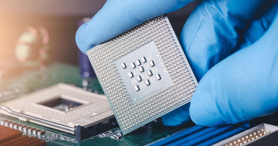


抖音二維碼

Q Q二維碼

微信二維碼
點擊
然后
聯系
然后
聯系
電話熱線
13410863085Q Q

微信

- 郵箱