鑫景福致力于滿足“快速服務,零缺陷,輔助研發”PCBA訂購單需求。


行業新聞
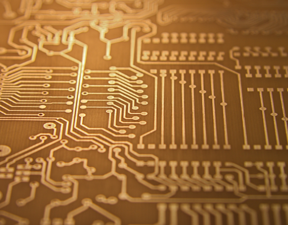
What is high-speed PCB design?
High Speed PCB design refers to any design whose signal integrity is affected by PCB physICal characteristics (such as layout, packaging, interconnection and layer stacking). Moreover, when you start to design circuit boards and encounter problems such as delay, crosstalk, reflection or EMIssion, you will enter the field of high-speed PCB design.

Due to the attention paid to these problems, high-speed design is so unique. You may be used to designing a SIMple PCB, focusing on the placement and routing of components. However, when using high-speed design, it is more important to consider some factors, such as their distance from the signal, the width of the signal, the location of the placement track and their types. Connected. In addition, considering these factors, it will reach a higher level in your PCB design process.
1. Know the design software that can provide advanced options
It needs a lot of complex functions to carry out high-speed design in CAD software. Also, there may not be many programs for amateurs, and there are usually no advanced options based on Web suites. Therefore, you need to have a better understanding of powerful CAD tools.
2. High speed routing
When high-speed routing is involved, designers need to understand the basic routing rules, including not cutting off the ground plane and keeping the routing short. Therefore, please prevent the digital line from crosstalk at a certain distance, and shield all interference generating factors to avoid damaging the signal integrity.
3. Routing with impedance control
For some signals of about 40-120 ohms, it requires impedance matching. The cue for characteristic impedance matching is the antenna and many differential pairs.
It is important that the designer knows how to calculate the routing width and the necessary impedance value of the stack. If the impedance value is incorrect, the signal may be seriously affected, resulting in data corruption.
4. Length matching trace
There are many lines in the high-speed memory bus and interface bus. These lines can operate at very high frequencies, so it is essential that signals be sent from the sending end to the receiving end at the same time. In addition, it needs a function calLED length matching. Therefore, the most common standards define the tolerance values that need to match the length.
High speed PCB design skills
5. Minimize loop area
High speed PCB designers need to know some skills. High frequency signals can cause EMI, EMC and other problems. Therefore, they need to follow basic rules, such as having a continuous ground plane and reducing the loop area by optimizing the current return path of the routing, as well as putting in many suture vias.
High Speed PCB design considerations
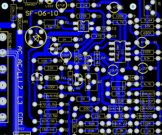
PCB layout is very important
Undoubtedly, efficient PCB manufacturing in high-speed circuits is very important for the final results. However, PCB layout is not considered in this process. Therefore, it will have a significant impact on the design to achieve the necessary functions and successfully carry out PCB manufacturing, such as high-level planning and compliance with important factors. In addition, you need to deal with some problems before PCB layout, such as the practice of manufacturing design (DFM) and additional consideration of high-speed PCB requirements.
Poor layout can cause performance problems when starting testing or for PCB manufacturing. Worse, because PCB failures or performance problems need to be evaluated and prototype layouts need to be reassembled, more cost and time will be spent on redesign or rework.
PCB Design Considerations
In fact, high-speed PCB design has many restrictions on designers, because you need to meet the requirements of various signal speeds and other designs. Therefore, to achieve the high-speed circuit board design shown below, some factors need to be considered:
Note on schematic diagram: As we all know, a good schematic diagram can lay a good foundation for PCB design. Therefore, depending on whether you are a PCB designer or an electrical engineer, you can handle schematic diagrams differently. In general, it views schematics as a means of communication that can be connected to a circuit board. But schematics can have a big impact on organizing and presenting your high-speed design. Therefore, there is as much information available on the design schematic as possible, such as routing length, necessary component placement, PCB manufacturer information, etc.
Trace length adjustment: When using high-speed interface, you need to adjust the trace length to synchronize signal transmission with data lines. However, the interface may fail at the maximum frequency, or it may not work at all because it is not synchronized. Moreover, the higher the interface frequency, the higher the length matching requirements. Therefore, in the case of parallel interfaces, you only need to adjust the length of all routes. It is important to adjust the length of these routes to obtain the required length in a group of signals.
High speed PCB design considerations
PCB materials and requirements for high-speed stacking: This will affect your high-speed design, such as the structure of layer stacking and PCB materials.
High speed placement strategy: Since changing pad size and component gap can minimize the high-speed connection length, it can use a variety of methods for high-speed design to optimize component placement and improve the occupied area of components to achieve high-speed.
Differential pair routing and routing length routing: It is very important to route differential pairs in high-speed design, so that paired signals can exist at the same time.
Crosstalk, impedance control and parallelism considerations: In high-speed design, there are many factors that will adversely affect your design. In addition, some techniques need to be considered, such as how to minimize the impact on the design.
Understand striplines and microstrip lines: Generally, for high-speed design, it requires a variety of methods to route wires. If you want to achieve high-speed routing, you'd better have a better understanding of stripline and microstrip routing technologies.
Cabling topology and best cabling practices: Generally, if you want to achieve the circuit path required for high-speed cabling, you need to use a specific shape or topology. Moreover, it is very good to explore various methods to track the route length, escape character, return path, etc.
Simulator: For high-speed design, simulation will bring great benefits before, during and after the layout. Therefore, you should have a better understanding of PCB design software to learn tips and techniques for simulation design.
How do I know if you need high-speed PCB design?
1. Is there a high-speed interface on the board?
A quick way to find out whether you need to follow the high-speed design guidelines is to check whether you have high-speed interfaces, such as DDR, PCI-e, or even video interfaces, such as DVI, HDMI, etc.
All these interfaces need to follow some high-speed design rules. In addition, please provide the exact specification of each data in the document.
2. Ratio of trace length to signal wavelength
Generally, if the wavelength of your MESsage is the same as the routing length, your PCB will definitely need high-speed design. Because some standards (such as DDR) require that the length of the routing match the minimum tolerance.
A good rough number is if your routing length and wavelength can be controlled within an order of magnitude of each other. Then, it is better to check the high-speed design.
How to know if you need high-speed PCB design
3. PCB with wireless interface
As you know, each PCB has an antenna, whether through connectors or things on the board, you need to design high-speed signals. In addition, the vehicle antenna also needs a tight impedance to match the tuning length.
For circuit boards with SMA connectors or similar connectors, you need to connect them to connectors with specific impedance values.
What determines the quality of PCB?
10-25,2022


抖音二維碼

Q Q二維碼

微信二維碼
點擊
然后
聯系
然后
聯系
電話熱線
13410863085Q Q

微信

- 郵箱