鑫景福致力于滿足“快速服務(wù),零缺陷,輔助研發(fā)”PCBA訂購單需求。


行業(yè)新聞
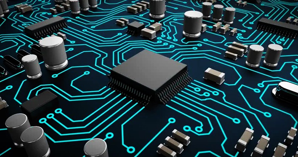
Circuit board manufacturers help you sort out the past, present and future of mICroelectronic component packaging
Since the 20th century, with the rapid development of computer and other communication industries, the microelectronics industry has gradually become an important industry in the world. At the same time, the microelectronics industry is also an important pillar industry in China. Now the microelectronics we are talking about has gradually separated into three independent pillar industries of design, manufacturing and packaging. With the continuous development of the microelectronics industry in recent years, the microelectronics packaging technology has become an important technology in the IT industry and an important part of the microelectronics industry.
The so-calLED microelectronic packaging technology refers to the assembly of many semiconductor electronic components into a complete package, and the power supply is provided by the outside world. Microelectronic packaging can ensure that IC can effectively avoid external interference during normal operation. Therefore, microelectronic packaging must meet the design requirements on Electronic devices and meet the requirements of various indicators in terms of quality and reliability.
The development of microelectronic packaging
There are many kinds of microelectronic packaging technology, which can be divided into through hole and surface mount according to the packaging mode. We divide the development of microelectronic packaging technology into three stages:
In the first stage, in the 1970s, the microelectronic packaging technology was mainly plug-in packaging technology. By the late 1970s, it had developed into dual in-line packaging technology, which can be applied in many places, such as molded ceramics.
In the second stage, in the 1980s, its main microelectronic packaging technology was Surface Mount Technology. In this period, its packaging technology was relatively mature. However, due to the defects in the lead arrangement of surface mount technology, it would be very difficult to keep all the leads on the surface coplanar. In order to solve the shortage of this packaging technology, another new microelectronic packaging technology has emerged, which is microelectronic lead flat packaging technology. Compared with plug-in packaging technology, this technology has greatly reduced the package size and operation difficulty.
In the third stage, in the 1990s, with the development of the tiMES, the continuous development of electronic technology and the continuous progress of integrated circuit technology, many new technologies were emerging, which made the requirements for the existing microelectronic packaging technology more strict. At the same time, there was the development from the original quad lead packaging technology to the planar packaging technology. This packaging technology beCAMe a more widely used packaging technology at that time, Until the late 1990s, with the continuous innovation of packaging technology, and after a long period of development, the current microelectronic packaging technology has gradually developed towards miniaturization and low power consumption.
Surface Packaging Technology
Now the microelectronic packaging technology mainly uses the brazing technology. Its main working principle is to solder the electronIC components on the surface to the designated bonding pad, so that the circuit function with reliability can be realized between these components and the bonding pad. Brazing mainly has the following two characteristics:
The surface assembly technology adopts the soft soldering technology. The brazing flux can effectively remove the impurities on the metal surface, so that the solder can play a certain role in lubrication.
The metal substance can be effectively formed between the brazing metal and filler metal, which makes it easier and faster in the packaging process.
chip level interconnection technology
Chip level interconnection technology is the basis of electronic packaging technology and plays an important role in electronic packaging technology. Both chip assembly and electronic packaging technology operate on the substrate, so these can be applied to interconnected micro technologies. In this way, micro interconnection technology is the core of packaging technology.
The current micro interconnection technologies mainly include the following:
① Wire bonding technology, the so-called wire bonding technology, its main work content is to connect the semiconductor chip with the outside of the electronic packaging by using certain means. The carrier automatic welding technology is a kind of interconnection technology with high level. Its main technical content is to make the corresponding pin with the required polymer according to the conductor drawing.
② Put the corresponding chip into the corresponding bonding area, and finally bond all the leads to the current position orderly through the thermoelectric electrode. The carrier automatic welding technology is relatively mature compared with other technologies, and its main advantages are low production cost and SIMple operation.
③ Flip chip technology is the main technology in packaging nowadays. Its main feature is that the chip is directly inverted on the corresponding substrate. The main advantage of this technology is that the solder joint can be placed anywhere on the chip, which greatly improves the utilization of the chip. Therefore, flip chip technology plays a vital role in microelectronic packaging technology.
summary
Microelectronic packaging technology has experienced several development stages, including cartridge packaging, surface mount packaging, narrow pitch surface mount, solder ball array packaging, and chip size packaging. At present, the most popular microelectronic packaging technologies are surface mount packaging and chip size packaging because of their low cost and easy operation. The overall development direction of surface mount solder ball array packaging is to gradually adopt lead-free soldering, which is helpful to protect the environment. At the same time, the volume of electronic devices is also gradually SMAller. In addition, the number and difficulty of installation also increase, so the reliability of packaging technology has now become a new research topic.

SOP Operation of PCBA Factory Staff
10-26,2022


抖音二維碼

Q Q二維碼

微信二維碼
點(diǎn)擊
然后
聯(lián)系
然后
聯(lián)系
電話熱線
13410863085Q Q

微信

- 郵箱