鑫景福致力于滿足“快速服務,零缺陷,輔助研發”PCBA訂購單需求。


行業新聞

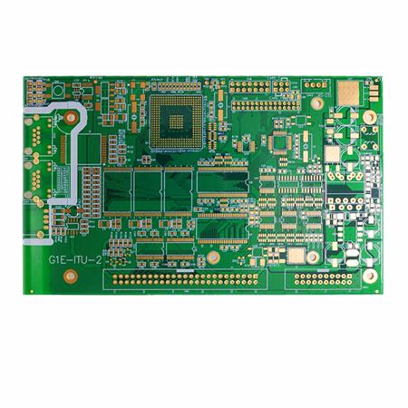
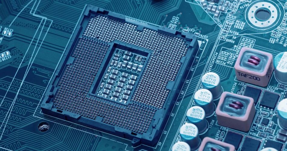
Due to the increase of integrated circuit package density, multilayer PCB leads to a high concentration of interconnects, whICh makes the use of multiple substrates necessary. Unforeseeable design problems such as noise, stray capacitance and crosstalk have occurred in the layout of printed circuit. Therefore, PCB design must focus on minimizing signal line length and avoiding parallel lines. Obviously, in a single panel, or even a double-sided panel, these requirements cannot be satisfied because of the limited number of intersections that can be realized. In the case of a large number of interconnection and cross requirements, if the circuit board wants to achieve a satisfactory performance, it must expand the board layer to more than two layers, so there is a multilayer circuit board. Therefore, the original intention of manufacturing multilayer circuit boards is to provide more freedom to select appropriate wiring paths for complex and/or noise sensitive electronic circuits.

The multilayer PCB circuit board has at least three conductive layers, two of which are on the outer surface, and the remaining one is synthesized in the insulating board. The electrical connection between them is usually realized through the plated through-hole on the cross section of the circuit board. Unless otherwise specified, multilayer printed circuit boards are generally plated through hole boards, just like double-sided boards. Multi substrate is made by stacking two or more layers of circuits with each other, and they are connected with each other reliably and preset. Since drilling and electroplating have been completed before all layers are rolLED together, this technology violates the traditional manufacturing process from the beginning. The innermost two layers are composed of traditional double-sided boards, while the outer layers are different. They are composed of independent single panels. Before rolling, the inner substrate will be drilled, through hole plated, pattern transferred, developed, and etched. The outer layer of the drilled hole is the signal layer, which is plated through by forming a balanced copper ring at the inner edge of the through-hole. The layers are then rolled together to form a multi substrate, which can be interconnected (between components) using wave soldering. Rolling may be done by hydraulic press or in overpressure chamber (autoclave). In the hydraulic press, the prepared materials (for pressure stacking) are placed under cold or preheated pressure (materials with high glass transition temperature are placed at a temperature of 170-180 ℃). The glass transition temperature is the temperature at which the amorphous region of amorphous polymer (resin) or part of crystalline polymer changes from a hard, rather brittle state to a viscous, rubbery state.
Multi substrate is put into use in professional electronic equipment (computers, military equipment), especially when the weight and volume are overloaded. However, this can only be achieved by increasing the cost of multiple substrates in exchange for increasing the space and reducing the weight. In high-speed circuits, multiple substrates are also very useful. They can provide more than two layers of boards for PCB designers to lay wires and provide large grounding and power supply areas.


抖音二維碼

Q Q二維碼

微信二維碼
點擊
然后
聯系
然后
聯系
電話熱線
13410863085Q Q

微信

- 郵箱