鑫景福致力于滿足“快速服務(wù),零缺陷,輔助研發(fā)”PCBA訂購單需求。


PCBA加工
PCBA Processing Automation Production requirements
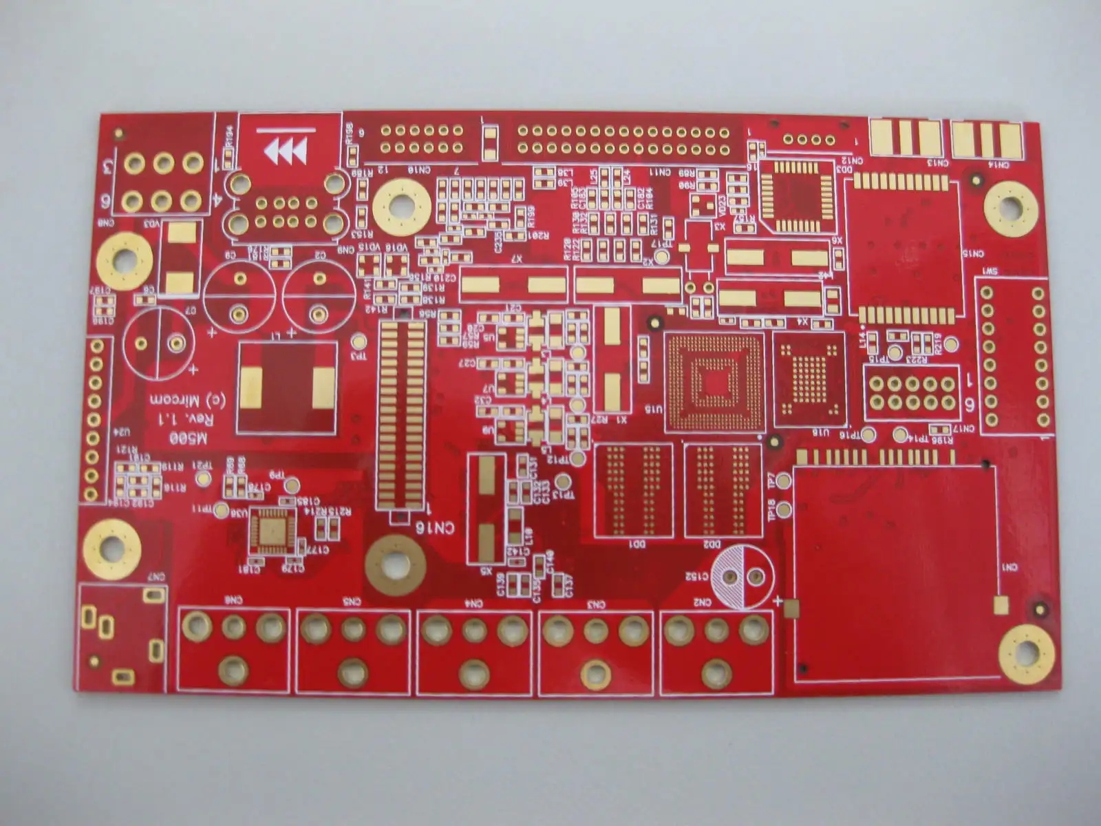
1. PCB size
[Background Description]
The size of PCB is limited by the capability of electronIC processing production line equipment. Therefore, proper PCB size should be considered in the design of product system scheme.
(1) The maximum PCB size that SMT equipment can mount coMES from the standard size of PCB sheet, most of which are 20 ″ × 24 ″, i.e. 508mm × 610mm (rail width)
(2) The recommended size is the size of each equipment in the SMT production line, which is conducive to giving play to the production efficiency of each equipment and eliminating equipment bottlenecks.
(3) For SMAll size PCB, it should be designed as a combination to improve the production efficiency of the whole production line.
Design Requirements
(1) Generally, the maximum size of PCB shall be limited to 460mm × Within 610mm.
(2) Recommended size range is (200~250) mm × (250~350) mm, the length width ratio should be<2.
(3) For dimensions<125mm × PCB of 125mm shall be assembLED into proper size.
2. PCB profile
[Background Description]
SMT production equipment uses rails to transfer PCBs, and cannot transfer irregular shaped PCBs, especially those with notched corners.
Design Requirements
(1) PCB shape shall be regular square with rounded corners.
(2) In order to ensure the stability of the transmission process, irregular shaped PCBs should be converted into standard squares by means of patching. In particular, the corner gaps should be filled to avoid jamming during the transmission of wave soldering grippers.
(3) The pure SMT plate is allowed to have a notch, but the notch size should be less than one third of the length of the side where it is located. For those exceeding this requirement, the design process side should be supplemented.
(4) The chamfering design of golden finger requires chamfering at the insertion side, and the two sides of the insertion plate should also be designed (1~1.5) × 45 ° chamfer to facilitate insertion.
3. Transport side
[Background Description]
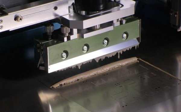
The size of the transmission side depends on the requirements of the transmission guide rail of the equipment. For the printing machine, the mounting machine and the reflow welding furnace, the transmission side is generally required to be more than 3.5mm.
Design Requirements
(1) In order to reduce PCB deformation during welding, the long side direction of non assembled PCB is generally taken as the transmission direction; The long side direction shall also be used as the transmission direction for the composition.
(2) Generally, the two edges of PCB or plate assembly transmission direction are used as the transmission edge. The minimum width of the transmission edge is 5.0mm. There should be no components or solder joints in the front and back sides of the transmission edge.
(3) There are no restrictions on SMT equipment at the non transmission side. It is better to reserve a 2.5mm element forbidden layout area.
4. Locating hole
[Background Description]
Many processes, such as plate assembly, assembly and testing, require accurate PCB positioning, so generally, positioning holes are required to be designed.
Design Requirements
(1) Each PCB shall be designed with at least two positioning holes, one designed as a circle, and the other designed as a long groove. The former is used for positioning, and the latter is used for guiding.
There is no special requirement for the positioning hole diameter. It can be designed according to the specifications of the factory. The recommended diameters are 2.4mm and 3.0mm.
Locating holes shall be non-metallic. If the PCB is a blanking PCB, the locating hole should be designed with a hole plate to enhance the rigidity.
The length of the guide hole is generally 2 times of the diameter.
The center of the positioning hole should be more than 5.0mm away from the transmission edge, and the two positioning holes should be as far away as possible. It is recommended to arrange them at the opposite corners of the PCB.
(2) For mixed PCB (PCBA with plug-in installed), the location of the positioning hole should be consistent, so that the front and back of the tooling can be shared, and the bottom bracket with screws can also be used for the tray of the plug-in.
5. Locator
[Background Description]
Modern mounters, printers, optical inspection equipment (AOI), Solder Paste Inspection equipment (SPI), etc. all use optical positioning systems. Therefore, optical positioning symbols must be designed on the PCB.
Design Requirements
(1) Positioning symbols are divided into global positioning symbols (Global Fiducial) and local positioning symbols (Local Fiducial). The former is used for the positioning of the whole board, and the latter is used for the positioning of the assembled sub boards or fine pitch components.
(2) The optical positioning symbol can be designed as a square, diamond shaped circle, cross shaped, well shaped, etc., with a height of 2.0mm. It is generally recommended to design a circular copper definition figure with a diameter of 1.0m. In consideration of the contrast between the material color and the environment, a non blocking welding area 1mm larger than the optical positioning symbol should be reserved. No characters are allowed in it. Whether there is copper foil in the inner layer of the three symbols on the same board should be consistent.
(3) On the PCB surface with SMD components, it is recommended to lay three whole board optical positioning symbols at the corners of the board to facilitate the three-dimensional positioning of the PCB (three points determine a plane, which can detect the thickness of solder paste).
(4) For the assembly, in addition to three optical positioning symbols for the whole board, it is better to design two or three optical positioning symbols for the assembly at the opposite corners of each unit board.
(5) For QFP with lead wire center distance ≤ 0.5mm and BGA with lead wire center distance ≤ 0.8mm and other devices, local optical positioning symbols shall be set at the opposite corners to facilitate accurate positioning.
(6) If there are mounted components on both sides, each side should have an optical positioning symbol.
(7) If there is no positioning hole on the PCB, the center of the optical positioning symbol shall be more than 6.5 mm from the transmission side of the PCB. If there is a positioning hole on the PCB, the center of the optical positioning symbol shall be designed on the side where the positioning hole is close to the center of the PCB.
What is circuit board assembly?
10-27,2022


抖音二維碼

Q Q二維碼

微信二維碼
點(diǎn)擊
然后
聯(lián)系
然后
聯(lián)系
電話熱線
13410863085Q Q

微信

- 郵箱