鑫景福致力于滿足“快速服務(wù),零缺陷,輔助研發(fā)”PCBA訂購單需求。


PCBA加工
Dimensions of PCBA pads and design defects of chip components
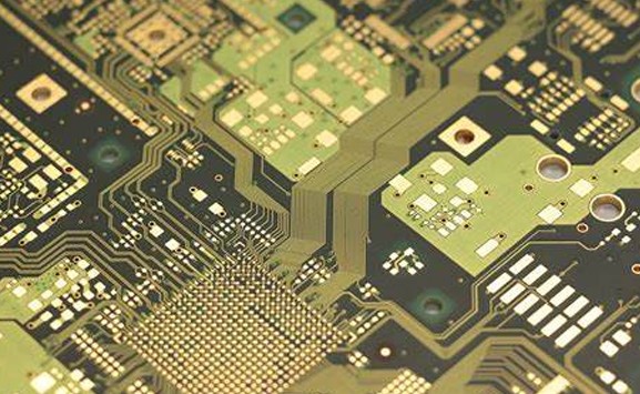
An important part of PCBA design is the SMT pad. The pad determines the position of components on the PCBA board, and directly affects the reliability of PCBA processing solder joints and welding defects, clarity, testing and maintenance in the process of processing. Therefore, the pad design will directly affect the manufacturability of the whole PCBA processing.
For SMT chip components, pad design is also crucial. In the design, we need to consider whether the amount of solder can meet the reliability of our joint parts, and whether it will lead to such undesirable phenomena as bridging and warping in the reflow process of PCBA processing. The matching between SMC/SMD and pad must meet the requirements of JB3243 and PC-7351.
The most common defects in the size design of PCBA pads are size errors, incorrect spacing, asymmetry, etc. These defects are likely to lead to such undesirable phenomena as false soldering, displacement, monument, and lack of tin during the welding process of SMT processing, whICh will affect the reliability of our boards.
The design defects of SMT chip component pads are as follows:
1. The QFP pad is too long, resulting in a short circuit.
2. The PLCC socket pad is too short, resulting in faulty soldering of the board.
3. Too long IC pad leads to too much solder, which leads to short circuit in reflow link.
4. The wing chip pad is too long, which affects the heel solder filling, and the heel is not well wetted.
5. The pad length of chip components is too short or too short, resulting in such phenomena as displacement, open circuit and inability to weld, which affect processing.
6. Affect the shape of solder joints and reduce the reliability of solder joints.
7. The pads processed by PCBA may be directly connected with a large area of copper foil, which may also lead to defects such as monument, faulty soldering, etc.
Shenzhen old brand electronic processing factory can provide you with high-quality SMT chip processing and PCBA processing, a real one-stop electronic processing service.


抖音二維碼

Q Q二維碼

微信二維碼
點(diǎn)擊
然后
聯(lián)系
然后
聯(lián)系
電話熱線
13410863085Q Q

微信

- 郵箱