鑫景福致力于滿足“快速服務,零缺陷,輔助研發”PCBA訂購單需求。


PCBA加工
SMT PCBA assembly design document
For the smooth transfer of products, this paper will focus on introducing the basIC documents that should be available when transferring general Circuit board assembly (PCBA).
Some companies have poor document control. Even the most basic circuit board (PCB) files are short of each other. For the smooth transfer of products, the following describes the basic files that should be available for general circuit board assembly (PCBA) transfer.
1. Gerber file or PCB CAD file
Gerber file is the most basic file for PCB manufacturing. When PCB factories receive Gerber files and import them into CAM software, they can provide production data for each PCB process. Gerber data can also provide image data for specific equipment, such as automated optical inspection equipment (AOI), and can also be used to define the basis for PCB steel plate aperture.
2. fab drawing (manufacturing standard)
This specification generally requires the PCB manufacturer to complete a piece of circuit board, so the following information is usually indicated on it. The circuit board assembly factory also usually uses this specification as the basis for inspection during incoming inspection:
Color of insulating printing ink. They are generally green, but also black and red.
Screen printing ink color. Generally, they are white and yellow, and other colors are rare.
Surface Finished of PCB, such as ENIG, HASL, OSP, etc. Some ENIGs also specify the thickness of gold and nickel layers, and some even specify the thickness of copper foil.
Base material grade of the circuit board. Current circuit boards are divided into lead and lead-free processes. The lead-free process requires high temperature resistance. When necessary, it is better to specify the Tg value (above 150C lead-free), Td value (above 325C lead-free) and Z-axis expansion coefficient (below 300ppm/degree) of FR4 substrate.
Electrical characteristics of copper foil. Especially high-frequency products.
V-cut and additional machining or drilling information.
Panel style and size.
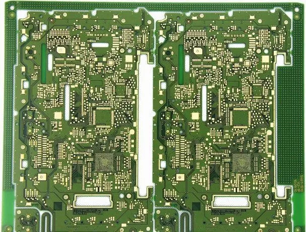
3. Panel drawing
The Gerber document above only defines the data of a single PCB, but in general, in order to improve the utilization rate of the circuit board and the efficiency of the manufacturer, the actual output of the circuit board is designed by splicing/connecting boards. The shape, style and size of the splicing board will affect the design of the following fixtures, and different splicing methods may even make the original fixture unusable:
Steel plate (Stencil)
Vacuum block
Visual Inspection template
MDA (Manufacturing Defect Analyzer) or ICT (In Circuit Tester) test fixture
FVT (Function Verification Tester)
When transferring from different production lines and factories, remember to use the original panel style. If the panel style is not defined in the original document, you can ask the original Circuit board manufacturer for it, and then standardize it.
4. Placement Component X-Y table
The SMT printing machine determines the position of the part on the circuit board according to the X and Y coordinate axes defined by the user. Of course, there are other parameters (Z axis, rotation...) to form the SMT printing program. The circuit board designer can generate an X and Y coordinate table of the part through PCB CAD, which can greatly reduce the time for SMT engineers to write programs.
If there is no way to generate X and Y coordinate tables from PCB CAD, you can still use the traditional method to slowly measure parts one by one with the projector, or open the Gerger document to measure on the computer. However, no matter which method is used to measure the results, the actual SMT machine will still need to fine tune when printing to conform to the actual coordinates.
5. Readable plots file
Most people may not be able to directly understand Gerber's files. Generally, we will output each layer of PCB as a readable PDF document, including solder paste layer, silk screen layer, shielding layer and each circuit layer.
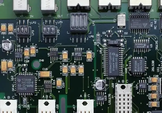
6. PCB assembly drawing
Generally speaking, today's circuit board assembly is based on the BOM (parts list), but occasionally there are still some additional jumpers or there is no way to use the BOM and part position indicators to specify. Therefore, PCB Assembly drawing is usually used to define how the factory completes the assembly of the whole circuit board after SMT or plug-in. For example, MARKing the part number of the circuit board after assembly, additional dispensing, etc.
7. Schematic drawing
Schematics are generally used by electronic engineers or repair technicians to repair circuit boards for reference. SometiMES they also use circuit diagrams to design test jigs.


抖音二維碼

Q Q二維碼

微信二維碼
點擊
然后
聯系
然后
聯系
電話熱線
13410863085Q Q

微信

- 郵箱