鑫景福致力于滿足“快速服務,零缺陷,輔助研發(fā)”PCBA訂購單需求。


PCBA加工
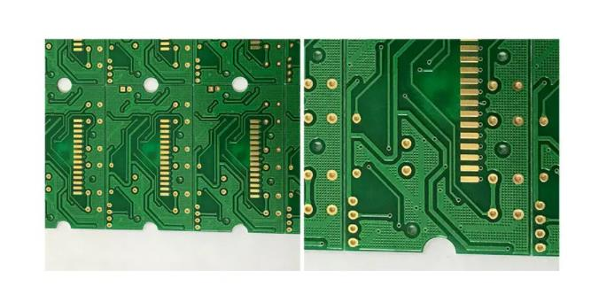
PCB order
PCB board customization refers to the circuit board manufacturers, according to the design drawings provided by the customer, SMAll batch of circuit board production. ScheduLED to make pcb circuit board products. Its production process and general circuit board production material difference.
PCB custom process
File--Project--PcBproject opens a Project.
File--New Create a New schematIC. To import a known file, file--open.
Draw Sch, where the Panel on the side of the window can be set in View. (Import Sch library and PCB library of all originals at the same time.)
Each component must be imported into the corresponding library to Place.
If you don't have one, add it to a mostly used folder and draw a schematic. Library --libraries--Project--Add lib-- Add mostly used libraries (Schlib and PCBlib) to the Project library. Then press the Add key in the SCH Library window (possibly from the Panel below) to Add the original, and the same goes for adding the PCB board package. Finally, press Edit in the schematic diagram lib of the original to associate the PCB package with the original.
After drawing the schematic diagram, MARK the package of each component and chip, give the number of each component, and give the value of each component.
Automatic labeling of components: Annotate Schematics Select Annotate Schematics in the Order of Processing and then Update Change List--Accepted Changes--Execute Changes--OK.
If the components are too crowded, you can enlarge the drawing by right-clicking Option-- Documnet Option-- Standard style.
The following are some rules for PCB custom drawing:
Create a new PCB file and save it (note that it can be renamed only when saved). Import PCB original library (in 09, PCB library and Sch library are the same Compile library, only the newly added libraries need to be imported).
Design--Update to PCB-- Execute Changes Import to PCB. Delete the green web after you import it.
If you want to change your original package, right click --find SIMilar Objects. If you find these objects, you can change their package in a similar way.
After drawing the new package, Update PCB Library, Update Sch to PCB.
Design--Rules Rules for PCB layout.
Tools--Design Rule Check allows you to perform Rule checks.
The horizontal and vertical distances between horizontal and vertical inserts should also be 100mile integer multiples. (1 mil = 0.0254 mm)
In general, the crystal oscillator should be close to the chip, and the indicator light should be placed on the front.
R--M ranging, E--D delete, P-- original, TAB view or modify original properties.
Design--board Layers&Colors changes layer properties
Click on the Original -PCB inspector- to change the various attributes of the original.
Pad belongs to Multilayer, and the size of the Pad through hole (aperture) is set to 40mil
The Via hole, which can be set in any Net, can be set before the corresponding Net can connect to the Via
The chip pin should be drawn from the chip.
The crystal vibration lead is as short as possible, the following is best not to take the line, can use GND to surround, power supply principle crystal vibration as far as possible.

The inner diameter of the pin is > 38mil, the outer diameter is > 70mil, and the diameter of other holes is > 30mil
The direction of JTAG should be noted. If you want to take the mirror image of a component, you take the mirror image of x that's symmetric about x, and you take the mirror image of y that's symmetric about y.
The Q key converts units
Via has a minimum internal meridian of 15mil and external diameter of 30mil.
The power supply and reset module are placed at the corner.
Keep the clock line as short as possible.
Add a teardrop before covering the floor.
Export PCB4.0 to Protel 99SE and open it again. By checking DRC, in the Browse PCB on the left of PCB boarddiagram, we can quickly locate where the mistakes were. Choose Violations in the Browse column, and then select the required mistakes in Violation column, and then Jump.
Add boundaries and mounting holes (inside = outside = 3mm) at the Keep Out Layer. If you want to assemble the board, draw the Mosaic pattern on the Keep out layer. Export PCB version 4.0 or 3.0.
Open the PCB you just exported in 99 and automatically save a 99 DDB. After overlying the land, DRC checks to ensure that there is no Violation or undesired Subnet. Export PCB2.8 ASCII. After exporting ASCII, DRC test must be carried out again, because if PCB is drawn in 09, some Mechanical layers will become Top Layer in ASCII due to packaging reasons, leading to unended short circuit. It is important to note that if there are elements in 09 that have green and purple layers, it is best to remove these layers in 09 first. The method of deletion is to Design--Make PCB Library based on the drawing of PCB. The system will create a PCB Library based on the original Library of the drawing, and then find the troublesome originals in the PCB Library and delete all Mechanical layers.
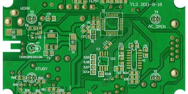
PCB customization skills
PCB board customization skills have a lot of, here can only simply say some circuit board customization skills, I hope to help you.
Set the Board of the PCB
Size: the Design - the Board Shape - Redefine Board Shape
Edit the Netlist: Right click --Option--Edit Netlist or Design--Net List --Edit Netlist.
Update From PCB Library after changing component Library: Tool--Update From PCB Library. Ctrl+Shift+ direction, the element can move a long distance. Eliminate errors T-M change the original layer mouse to the original L
If you find that many elements are labeled green in the diagram, you should change Rules or change the attributes of the element. If you don't think there is a problem with the layout, but you don't know what rules are causing the elements to turn green, you can remove the hook from the Enable TAB to find out what rules are wrong. If all components display only naMES but not values, we can select all components by finding similar Objects, and then select Show Comments in the PCB Inspector and remove the show name.
The Name of the component is written in the Name column, and the value is written in the Comment column, so that complete information can be obtained when the PCB is imported. To change the Name of each Pin, you can double-click the original in the schematic diagram, and then click Edit Pins to change the Name in the column of Name. The general Name can not be displayed on the diagram, so all the hooks in the column of Name on the far right are removed, and the Number is hooked to display the Pin Number.
Print to scale, page Setup --scale print Page Setup --Advance, layers can be selected. If the component package is found in the LIB but cannot be found when the PCB is imported, delete the original package in the component and then reload it


抖音二維碼

Q Q二維碼

微信二維碼
點擊
然后
聯(lián)系
然后
聯(lián)系
電話熱線
13410863085Q Q

微信

- 郵箱