鑫景福致力于滿足“快速服務,零缺陷,輔助研發”PCBA訂購單需求。


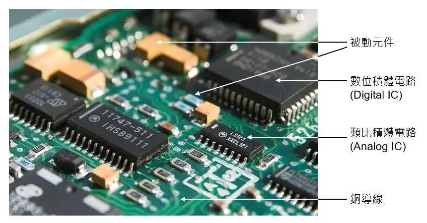
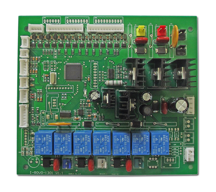
PCBA加工
Circuit board factory: explain SMT mounting process requirements in detail
With the continuous improvement of China's electronIC technology level, China has become the processing plant of the world's electronic industry. Surface Mount Technology is an important part of advanced electronic manufacturing technology. The rapid development and popularization of SMT processinghas played a unique role in promoting the development of contemporary information industry. At present, SMT has been widely used in the assembly of electronic product components and devices in all walks of life. Corresponding to the development status and trend of SMT, and the technical demand for SMT brought by the rapid development of information industry and electronic products, China's electronic manufacturing industry is in urgent need of a large number of professional and technical talents who master SMT knowLEDge.
Process Purpose
This process is to use the placement machine to accurately paste the chip components on the corresponding position of the PCB surface printed with solder paste or paster.
Patch process requirements
1、 Process requirements for mounting components
1. The type, model, nominal value, polarity and other characteristic MARKs of components with assembly tag number shall meet the requirements of assembly drawing and detailed list of products.
2. The mounted components shall be intact.
3. The welding end or pin of the mounted components shall be immersed in solder paste with a thickness of no less than 1/2. The amount of solder paste extrusion (length) shall be less than 0.2mm for general component mounting, and less than 0.1mm for narrow spacing component mounting.
4. The ends or pins of components are aligned and centered with the bonding pad graphics. Due to the self positioning effect during reflow soldering, certain deviation is allowed for the mounting position of components. The allowable deviation range requirements are as follows:
(1) Rectangular component: under the condition of correct PCB pad design, the width of the component in the width direction shall be more than 3/4 of the weld end width on the pad. After the component's weld end overlaps the pad in the length direction, the extension of the pad shall be greater than 1/3 of the height of the weld end; In case of rotation deviation, more than 3/4 of the component welding end width must be on the pad. Special attention shall be paid during mounting: the component welding end must contact the solder paste pattern.
(2) SMAll shape transistor (SOT): X, Y, T (rotation angle) are allowed to have deviation, but the pins (including toes and heels) must be all on the pad.
(3) Small outline integrated circuit (SOIC): X, Y, T (rotation angle) are allowed to have mounting deviation, but 3/4 of the device pin width (including toe and heel) must be kept on the bonding pad.
(4) Quadrilateral flatpack devices and ultra small package devices (QFP): It is necessary to ensure that 3/4 of the pin width is on the bonding pad, and small mounting deviation of X, Y, T (rotation angle) is allowed. The toe of the pin is allowed to extend out of the pad in a small amount, but 3/4 of the pin length must be on the pad, and the heel of the pin must also be on the pad.
2、 Three elements to ensure the mounting quality
1. Components shall be correct. The type, model, nominal value, polarity and other characteristic marks of components with assembly tag number shall conform to the requirements of the assembly drawing and list of products, and shall not be pasted in the wrong position.
2. Accurate position
(1) The ends or pins of components shall be aligned and centered with the solder pad graphics as far as possible, and the solder end of components shall be in contact with the solder paste graphics.
(2) The mounting position of components shall meet the process requirements.
The self positioning effect of the chip element at two ends is relatively large. When the element is mounted, more than 1/2 to 3/4 of the width direction of the element is lapped on the bonding pad. As long as the two ends in the length direction are lapped on the corresponding bonding pad and contacted with the solder paste pattern, they can self position during reflow soldering. However, if one of the ends is not lapped on the bonding pad or contacted with the solder paste pattern, displacement or suspension bridge will occur during reflow soldering.
The self positioning effect of SOP, SOJ, QFP, PLCC and other devices is relatively small, and the mounting offset cannot be corrected by reflow soldering. If the mounting position exceeds the allowable deviation range, it must be adjusted manually before entering the reflow welding furnace for welding. Otherwise, rework must be carried out after reflow welding, which will result in waste of man hours and materials, and even affect product reliability. If the mounting position exceeds the allowable deviation range during production, the mounting coordinates shall be corrected in time.
The manual mounting or manual alignment requires accurate mounting position, and the pins should be aligned and centered with the pads. Do not place them incorrectly Drag the solder paste to align it, so as to prevent the solder paste graphics from sticking and causing bridging.
3. The pressure (mounting height) should be appropriate. The mounting pressure (Z-axis height) should be appropriate. If the mounting pressure is too low, the welding end or pin of the component will float on the surface of the solder paste, and the solder paste will not stick to the component, which is easy to cause position movement during transfer and reflow soldering. In addition, because the Z-axis height is too high, the component will be dropped from a high place when mounting, which will cause the placement position offset; Excessive patch pressure and excessive solder paste extrusion are easy to cause solder paste adhesion. Bridging is easy to occur during reflow soldering. At the same time, the placement of the patch will shift due to sliding, and components will be damaged in serious cases.


抖音二維碼

Q Q二維碼

微信二維碼
點擊
然后
聯系
然后
聯系
電話熱線
13410863085Q Q

微信

- 郵箱