鑫景福致力于滿足“快速服務(wù),零缺陷,輔助研發(fā)”PCBA訂購單需求。


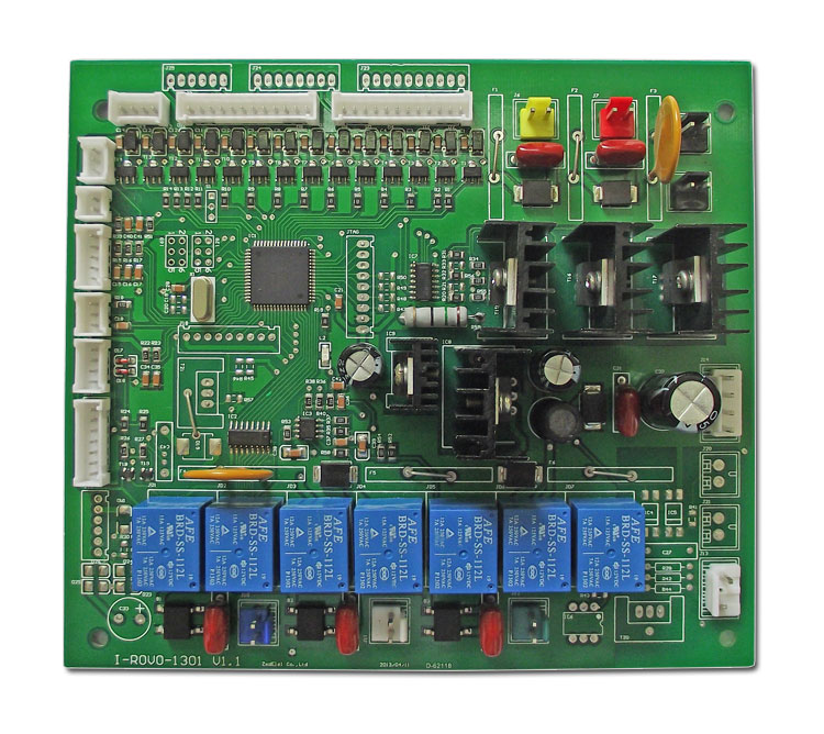
PCBA加工
DetaiLED explanation of incoming material inspection of SMT process flow
Since solder paste printing, operation of SMT machine and reflow soldering furnace welding should be listed as key processes in SMT process of PCB manufacturers, the incoming material inspection in SMT processing will be described first.
Inspection before assembly (incoming inspection)
1. Inspection method
The inspection methods mainly include visual inspection, automatIC optical inspection (AOI), X-ray inspection, ultrasonic inspection, online inspection, functional inspection, etc.
(1) Visual inspection refers to the method of inspecting the assembly quality directly with the naked eye or with the aid of magnifying glass, microscope and other tools.
(2) Automatic optical inspection (AOI) is mainly used for process inspection: solder paste printing quality inspection after printing machine, paste installation quality inspection after paste installation, and post weld inspection after reflow soldering furnace. AOI is used to replace visual inspection. X-ray inspection and ultrasonic inspection are mainly used for BGA, CSP, and Flip chip solder joint inspection.
(3) On line test equipment adopts special isolation technology to test resistance value of resistor, capacitance value of capacitor, inductance value of inductor, polarity of components, short circuit (bridge), open circuit (open circuit) and other parameters, automatically diagnose errors and faults, and display and print them.
(4) The function test is used for the electrical function test and inspection of the surface mount plate. The function test is to assemble the surface of the board or table. The unit to be tested on the surface assembly board inputs electrical signals as a functional body, and then detects the output signals according to the design requirements of the functional body. Most functional tests have diagnostic procedures, which can identify and determine faults. However, the equipment for functional testing is expensive. The SIMplest function test is to connect the surface assembly board to the corresponding circuit of the equipment for power on to see whether the equipment can operate normally. This method is simple and requires less investment, but it cannot automatically diagnose faults.
The specific method shall be determined according to the specific conditions of SMT production line of each unit and the assembly density of surface mount plate.
2. Incoming inspection
Incoming inspection is the primary condition to ensure the surface assembly quality. The quality of components, printed circuit boards and surface assembly materials directly affects the assembly quality of surface assembly boards. Therefore, the electrical performance parameters of components and the solderability of welding terminals and pins; Productive design of printed circuit board and solderability of bonding pad; The quality of surface assembly materials such as solder paste, patch adhesive, bar solder, flux, cleaning agent, etc. shall be subject to strict incoming material inspection and management system.
3. Inspection of surface mounted components (SMC/SMD)
The main inspection items of components: solderability, pin coplanarity and usability shall be sampled by the inspection department. The solderability of components can be tested by clamping the component body with stainless steel tweezers and immersing it in a tin pot at 235 ℃± 5 ℃ or 230 ℃± 5 ℃, taking it out after 2 ± 0.2s or 3 ± 0.5s, and checking the tin sticking on the welding end under a 20 fold microscope It is required that 90% of the soldering ends of the components are stained with tin. As a processing workshop, the following visual inspections can be carried out:
(1) Visually or with a magnifying glass, check the welding end or pin surface of components for oxidation and contamination
(2) The nominal value, specification, model, accuracy, overall dimensions, etc. of components shall conform to the product process requirements. (3) The pins of SOT and SOIC shall not be deformed, and the pin coplanarity of the multi lead device QFP with lead spacing less than 0.65mm shall be less than 0.1mm (optical detection by the mounting machine). (4) For the products requiring cleaning, the MARKs of components and parts shall not fall off after cleaning, and the performance and reliability of components and parts shall not be affected (visual inspection after cleaning).
(1) The layout and size of PCB pad, solder mask, wire MESh and through hole shall meet the design requirements of SMT printed circuit board. (For example, check whether the distance between pads is reasonable, whether the screen is printed on the pads, and whether the through hole is made on the pads)
(2) The overall dimensions of PCB shall be consistent, and the overall dimensions, positioning holes, datum marks, etc. of PCB shall meet the requirements of production line equipment.
(3) Allowable warping size of PCB:
① Upward/convex: maximum 0.2mm/5Omm length maximum 0.5mm/whole PCB length direction.
② Down/concave: maximum 0.2mm/5Omm length maximum 1.5mm/whole PCB length direction.
(4) Check the PCB for contamination or moisture


抖音二維碼

Q Q二維碼

微信二維碼
點(diǎn)擊
然后
聯(lián)系
然后
聯(lián)系
電話熱線
13410863085Q Q

微信

- 郵箱