鑫景福致力于滿足“快速服務,零缺陷,輔助研發”PCBA訂購單需求。


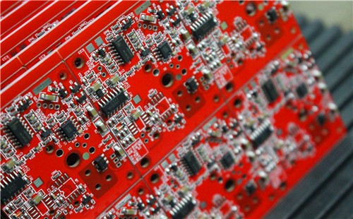
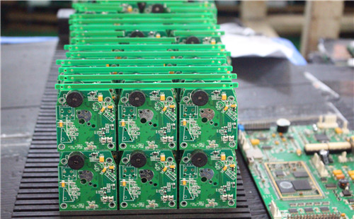
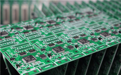
PCBA加工
Diagnosis and treatment of common printing defects in PCBA
In the process of PCBA processing, there are often some problems of poor printing, whICh is how to diagnose and deal with.
① Common understanding of poor printing.
② Diagnosis and treatment of tinning.
Phenomenon description: there is a little ink paste between the two welding pads. In high temperature welding, the main tin body on each pad is often pulLED back. If it cannot be pulled back, it will cause short circuit or solder ball, resulting in poor welding.
Diagnosis of tin bonding: less tin powder, low viscosity of tin powder, large particle size of tin powder, high room temperature, too thick printing, high placing pressure, etc.
Tin bonding treatment: increase the proportion of metal components in the solder paste; Increase the viscosity of solder paste; Reduce the particle size of tin powder; Reduce the temperature (below 270 ℃); Reduce the thickness of the printed solder paste (reduce to the overhead height, reduce the pressure and speed of the scraper); Enhance the accuracy of printing paste; Adjust various construction parameters of solder paste; Reduce the pressure exerted by part placement; Adjust the temperature curve of preheating and fusion welding.
③ Diagnosis and treatment of tin infiltration.
Phenomenon description: After printing, there is excess solder paste or burrs near the solder paste.
Tin penetration diagnosis: the scraper pressure is insufficient, the scraper angle is too SMAll, the steel plate opening is too large, the PCB and PAD size is too small, the printing is misaligned, the printer parameter setting is unreasonable, the PCB and the steel plate are not closely fitted, the solder paste viscosity is insufficient, the PCB or the bottom of the steel plate is not clean, etc.
Tin infiltration: adjust the parameters of solder paste printing; Clean or replace the template, clean or replace the PCB; Improve the accuracy of printing; Improve the viscosity of solder paste.
④ Diagnosis and treatment of solder paste collapse and powdery solder paste.
Phenomenon description: The solder paste is poorly formed on the PCB, the printing height is different, and the solder paste is powdery and granular.
Solder paste collapse Solder paste pulverization diagnosis: too much solvent in the solder paste, too much solvent when wiping the bottom of the steel plate, solder paste dissolved in the solvent, wiping paper does not rotate, solder paste quality is poor, PCB printing is placed in the air for too long, PCB temperature is too high.
Solder paste collapse Solder paste pulverization treatment: increase the proportion of metal components in the solder paste; Increase the viscosity of solder paste; Reduce the particle size of tin powder; Reduce the temperature (below 270 ℃); Reduce the thickness of the printed solder paste (reduce to the overhead height, reduce the pressure and speed of the scraper); Enhance the accuracy of printing paste; Adjust various construction parameters of solder paste; Reduce the pressure exerted by part placement; Avoid putting solder paste and printed PCB in wet air for a long time; Reduce the activity of flux in solder paste; Reduce the lead content in the metal.
⑤ Diagnosis and treatment of solder paste tip pulling.
Phenomenon description: The solder paste is poorly formed on the PCB, the SMEared area is too large, and the solder joint spacing is too small.
Solder paste sharpening diagnosis: the opening of steel plate is not smooth, the opening size of steel plate is too small, the demoulding speed is unreasonable, PCB solder joints are polluted, the solder paste quality is abnormal, and the steel plate is not cleaned.
Solder paste sharpening: clean or replace the steel plate; Clean or replace PCB; Adjust printing parameters; Replace the solder paste with good quality.
⑥ Diagnosis and treatment of tin deficiency.
Phenomenon description: insufficient solder paste on PCB.
Diagnosis of tin deficiency: unreasonable steel plate opening size, too thin plate mold, steel plate plug hole, steel plate pollution, unreasonable demoulding speed and method, etc.
Less tin treatment: increase the thickness of printing paste, such as cleaning or replacing the template; Adjust printing parameters; Improve printing accuracy.
⑦ Diagnosis and treatment of tin excess.
Phenomenon description: There is too much solder paste on the PCB solder pad.
Diagnosis of excessive tin: the opening size of steel plate is unreasonable, the plate mold is too thick, the room temperature is high, the printing is too thick, and the placing pressure is high.
Multi tin treatment: select the appropriate opening form; Reduce the thickness of printing paste; Adjust printing parameters; Improve printing accuracy.
⑧ Diagnosis and treatment of offset.
Phenomenon description: The printing solder paste deviates from the solder pad on the PCB.
Offset diagnosis: unreasonable opening position of steel plate, inaccurate PCB positioning, etc.
Offset processing: readjust the PCB printing positioning and replace the template to improve the printing accuracy.
PCB manufacturers, PCB designers and PCBA processors will explain the diagnosis and treatment of common poor printing in PCBA.


抖音二維碼

Q Q二維碼

微信二維碼
點擊
然后
聯系
然后
聯系
電話熱線
13410863085Q Q

微信

- 郵箱