鑫景福致力于滿足“快速服務,零缺陷,輔助研發”PCBA訂購單需求。


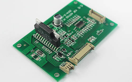
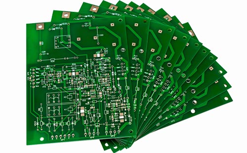
PCBA加工
DFM Analysis of Common PCBA Production Defects and PCBA Scheme design
PCBA production process involves a series of processes, whICh are complex and require close cooperation of all processes. Any problem in any link is likely to lead to welding defects of PCBA plates.
Common PCBA production defects include:
Missing parts, lack of tin, tin ball (tin bead), connected tin (short circuit), faulty soldering (empty soldering), tombstone, etc
1. Missing parts
The position of the mounting component on the PCB is missing.
2. Little tin
When solder paste is printed, due to factors such as too low scraper pressure and unsuitable steel MESh port, it is easy to miss the solder pad printed on the PCB, and the solder pad is oxidized during welding and the wave soldering is not adjusted properly, which is also easy to lead to less tin.
3. Tin ball
Solder balls are also calLED solder beads. Solder balls are left on PCB boards and component pins. Solder balls are easy to be generated due to poor printing of solder paste, improper setting of reflow temperature curve, and moisture in PCB.
4. Continuous tinning
Tin connection also refers to short circuit, which refers to the connection between two pins where there should be no tin connection, causing a short circuit. The collapse of solder paste during solder paste printing and poor wave soldering are easy to lead to the defect of connecting tin.
5. False welding
False soldering, also known as empty soldering and false soldering, refers to the unstable state that there is only a SMAll amount of tin connection at the solder joint, resulting in poor contact and intermittent interruption. When solder paste is printed, there is little tin, and the element floats high.
6. Erect a monument
A tombstone is also called a tombstone, which means that one end of the component is detached from the solder joint, causing it to stand upright. During reflow soldering, due to heating too fast, there is a temperature difference between the two ends of the element, one end of the solder is completely melted, and the other end is still in the melting state, which is easy to occur at this time.
The defects in PCBA production process are caused by many factors, which are not only related to the operation level of employees, but also related to equipment and accessories.
DFM Analysis of PCBA Scheme Design
DFM analysis of PCBA scheme design refers to the manufacturability analysis conducted by PCBA manufacturers to help customers' products go online for production. PCBA manufacturers will, based on years of processing experience, analyze the structure of PCB circuit boards, put forward suggestions for improvement, optimize the layout of circuits and components, make the production of products more consistent with the manufacturing process, and improve the quality and stability of products.
DFM analysis in PCBA scheme design has the following advantages.
1. Improve the yield of PCB production
Because electronic product design engineers do not understand the PCB production process, they only consider the realization of product functions when designing PCB, and easily ignore the difficulty of PCB production. Through DFM analysis of PCB structure, PCBA processing plants can help optimize the circuit, reduce the difficulty of PCB manufacturers' production, and improve the yield of PCB production.
2. Improve the yield of SMT/DIP
In SMT chip processing and DIP plug-in processing, the circuit distribution and component layout of PCB design have a very important impact on the yield and reliability of production. In the process of SMT chip processing, the smaller the PCB pads and components, the greater the difficulty of processing. Therefore, larger components should be selected when PCB size is determined and allowed. These details are easily ignored by PCB design engineers.
3. Easy maintenance
In PCB design, some components are arranged too closely. When electric soldering iron is used for maintenance, nearby components are easy to burn, which increases the difficulty of maintenance. Based on their years of processing experience, PCBA manufacturers can help engineers optimize circuits and components, making maintenance easier.
4. Reduce costs
A good PCB design is conducive to the processing and production of products and improves the yield of products. In addition, it can also reduce the cost of fixture production. If the SMD components and plug-in components are arranged separately, the manufacturing difficulty of the fixture can be reduced during wave soldering, and the processing cost can be finally reduced.
DFM analysis in PCBA scheme design can help customers better optimize the structure of PCB circuit board, better conform to online production, reduce production costs and improve quality. With the reduction of processing difficulty, it also helps to reduce the processing costs of customers.


抖音二維碼

Q Q二維碼

微信二維碼
點擊
然后
聯系
然后
聯系
電話熱線
13410863085Q Q

微信

- 郵箱