鑫景福致力于滿足“快速服務,零缺陷,輔助研發”PCBA訂購單需求。


PCBA加工

How to copy boards
In the absence of electronIC document production materials and only circuit board templates, in order to shorten the development time and save development costs, it is a very affordable way to use templates for copying and proofing. The following PCB company introduces the method of PCB copying:
The first step is to get a PCB. First, record the models, numbers, and positions of all components on the paper, especially the directions of the diode, the transistor, and the IC notch. It is better to take two photos of the position of the pneumatIC parts with a digital CAMera. The current circuit board is becoming more and more advanced, and the diode and triode on it are not noticeable.
The second step is to remove all devices and remove the tin in the PAD hole. Clean the PCB with alcohol, and then put it into the scanner. When the scanner scans, it needs to slightly increase the scanning pixels to get a clearer image. Then polish the top layer and bottom layer slightly with water gauze until the copper film is bright, put it into the scanner, start PHOTOSHOP, and sweep the two layers in color. Note that the PCB must be placed horizontally and vertically in the scanner, otherwise the scanned image cannot be used.

Step 3: Adjust the contrast and lightness of the canvas to make the part with copper film and the part without copper film have a strong contrast. Then turn the secondary image into black and white to check whether the lines are clear. If not, repeat this step. If the image is clear, save it as a black and white BMP file TOP.BMP and BOT.BMP. If you find a problem with the image, you can also use PHOTOSHOP to repair it.
Step 4, convert the two BMP files into PROTEL files, and call in two layers in PROTEL. If the positions of PAD and VIA passing through the two layers basically coincide, it indicates that the previous steps are well done. If there is any deviation, repeat the third step. Therefore, PCB board copying is a very patient work, because a SMAll problem will affect the quality and the matching degree after board copying.
Step 5: convert BMP of TOP layer into TOP PCB, pay attention to convert to SILK layer, which is the yellow layer. Then you can trace lines on TOP layer, and place devices according to the drawing in step 2. Delete SILK layer after drawing. Repeat until all layers are drawn.
Step 6: In PROTEL, call TOP.PCB and BOT.PCB, and combine them into a picture.
Step 7: Use the laser printer to print TOP LAYER and BOTTOM LAYER on the transparent film (1:1 ratio), put the film on that PCB, and compare whether there is any error. If it is correct, you will be finished. A copy of the original board was born, but it was only half finished.
We also need to test whether the electronic technical performance of the board is the same as that of the original board. If Yiyang is really finished. Note: If it is a Multilayer board, you should carefully polish it to the inner layer, and repeat the copying steps from step 3 to step 5 at the same time. Of course, the naMES of the figures are different, and they should be determined according to the number of layers. Generally, the copying of double-sided boards is much SIMpler than that of multilayer boards, and the multi-layer boards are prone to misalignment, so the copying of multilayer boards should be particularly careful and careful (the internal through holes and non through holes are prone to problems).
How to design PCB to meet factory assembly requirements
In the early days, PCB companies always thought that the design focus of FPC was to make the wiring layout well and the thickness of the stiffener under the golden finger right, so that FPC could not be inserted into the connector or loose because it was too thick. Later, it was occasionally found that FPC would break, especially when HotBar was working, it was found that the sections stacked with all materials could not be designed on the same vertical plane, so as to disperse stress concentration. Later, it was found that the copper foil of FPC had the so-calLED difference between rolled copper (RA) and electrolytic copper (ED), and the wrong copper foil would affect the life of FPC bending times, Later, it was found that electroplating copper was still used in the conduction process of more than two layers of rolled copper, which almost wiped out the characteristics of rolled copper. It seems like a lot of nonsense. As electronic products become smaller and smaller, FPC connectors become smaller and smaller. Although FPC does not necessarily become smaller, it seems to become larger, because it replaces some PCB functions, and the circuit seems to become denser. In addition, parts adjacent to FPC connectors become more and more close, which makes it more and more difficult to properly assemble FPC, Does your company have any special design to help operators confirm the FPC installation position? What design or foolproof can help the operator to easily and painlessly complete the installation of FPC? In fact, the following FPC designs can be seen in many mobile phone designs. Just put them forward for reference and see what other methods you can discuss.
1. The FPC installation indicator line is designed on the FPC. The FPC installation indicator line is just at the edge of the FPC after the FPC installation indicator line coupler cover is designed, which is helpful to judge whether the FPC is installed to the location. MARKing installation indicator lines on the front, rear and back of the FPC can help the operator judge whether the FPC has been correctly installed to the location. More attention will be paid to the design of two lines. When the FPC is installed to the location, the first indicator line will be covered by the coupler, while the second indicator line will remain outside the connector, so that the operator can more clearly judge whether there is installation deflection. Shenzhen Honglijie thinks that it is enough to have one indicator line, which should be visible after the connector cover.
2. Extend the length of the backless stiffening plate The backless stiffening plate can facilitate the capture of the FPC, allowing the operator to install the FPC into the connector more smoothly.
3. Design additional wings to add an additional small bump/wing/ear (TAB) on the left and right sides of the small FPC at the place where the FPC is close to the golden finger, so that the operator can easily grasp the FPC and install it into the connector, or design a "pick" small tool to hook the two small ears and slide the FPC into the connector.

How to ensure safety in chip processing
11-10,2022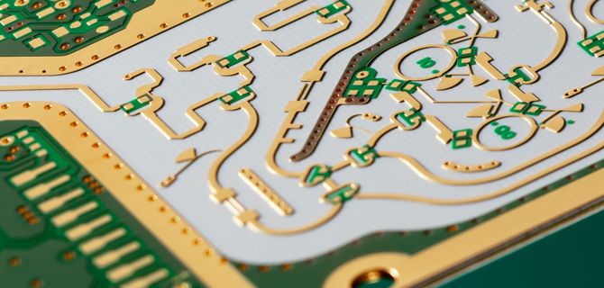


抖音二維碼

Q Q二維碼

微信二維碼
點擊
然后
聯系
然后
聯系
電話熱線
13410863085Q Q

微信

- 郵箱