鑫景福致力于滿足“快速服務,零缺陷,輔助研發”PCBA訂購單需求。


PCBA加工

How to Control the Quality of PCBA Processing
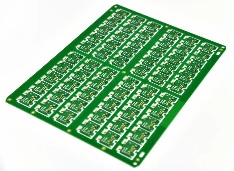
PCB company is a PCBA OEM manufacturer providing one-stop servICes for PCB board manufacturing, component purchasing, SMT chip processing, DIP plug-in processing, and PCBA testing. Next, we will introduce how to control the quality of PCBA processing? There are many links involved in the manufacturing process of PCBA, so we must control the quality of each link to produce good products. Generally, PCBA consists of a series of processes, such as PCB board manufacturing, component procurement and inspection, SMT chip processing, plug-in processing, program firing, testing, aging, etc. Let's elaborate on what needs to be paid attention to in each link.
1. After PCB board manufacturing receives the order from PCBA, analyze Gerber documents, pay attention to the relationship between PCB hole spacing and board bearing capacity, do not cause bending or fracture, and whether the wiring takes into account high-frequency signal interference, impedance and other key factors.
2. The purchase of components and parts and the inspection of the purchase of components and parts need to strictly control the channels. We must pick up the goods from large traders and the original factory, and 100% avoid second-hand and fake materials. In addition, special incoming material inspection posts shall be set up to strictly check the following items to ensure that components are free of failure. PCB: reflow soldering furnace temperature test, no flying wire, whether the via is blocked or leaks ink, whether the board surface is bent, etc; IC: Check whether the silk screen is completely consistent with the BOM, and store it at constant temperature and humidity; Other common materials: check silk screen, appearance, power on measurement value, etc. The inspection items are carried out according to the sampling method, and the proportion is generally 1-3%.
3. SMT assembly processing solder paste printing and reflow soldering furnace temperature control are key points, and it is very important to use laser steel MESh with good quality and meeting process requirements. According to the requirements of PCB, some of the steel mesh holes need to be increased or reduced, or U-shaped holes are used to make the steel mesh according to the process requirements. The temperature and speed control of reflow soldering furnace is very important for solder paste infiltration and welding reliability. It can be controlLED according to normal SOP operation guidelines. In addition, AOI detection needs to be strictly implemented to minimize defects caused by human factors.
4. In the process of DIP plug-in processing, the mold design of wave soldering is the key point. How to use the mold to maximize the probability of good products after the furnace is a process that PE engineers must constantly practice and summarize experience.
5. In the previous DFM report, it is suggested that customers should set some test points on PCB to test the continuity of PCB and PCBA circuit after all components are welded. If conditions permit, the customer can be asked to provide a program to burn the program into the main control IC through a burner (such as ST-LINK, J-LINK, etc.), so that the functional changes caused by various touch actions can be tested more intuitively, so as to check the functional integrity of the entire PCBA.
6. PCBA board test For orders with PCBA test requirements, the main test contents include ICT (In Circuit Test), FCT (Function Test), Burn In Test (Aging Test), temperature and humidity test, drop test, etc. The specific operation is based on the customer's test plan and the report data can be summarized.
How do engineers plan circuit board design
1、 Planning of power supply and floor number
The number of power supply layers is mainly determined by the number of power supply types, distribution, current carrying capacity, performance indicators of the board and the cost of the board. The setting of the power plane needs to meet two conditions: the power supply is not staggered; Avoid cross segmentation of important signals in adjacent layers. The following points should be paid attention to when setting the number of floors on the ground: the second floor corresponding to the main components should have a relatively complete ground plane; High speed, high frequency, clock and other important signals shall refer to the ground plane; The main power supply is tightly coupled to the ground plane, reducing the power plane impedance, etc.

2、 Signal layer planning
The wiring channel is usually an important factor in determining the number of signal layers. First, it should be clear whether there is a deep BGA and connector on the board. The depth of the BGA and the BGA PIN spacing are the key to determine the number of BGA outlet layers. For example, two lines can be passed between 1.0mm BGA vias, and only one line can be passed between 0.8mm BGA vias. There is a big difference in the number of outlet layers between the two. The connector mainly considers its depth, and basically a pair of differential lines pass between two vias. The BGA outgoing line between two vias can pass through two lines, the BGA outgoing line between two vias can only pass through one line, and the BGA outgoing line between two vias can only pass through one line. The BGA outgoing line between two vias can only pass through four routing layers. Secondly, the wiring channel of high-speed signal on the board should be considered. Because there are many conditions required for high-speed signal processing, it is necessary to consider such factors as stub, wiring spacing, reference plane, etc., so it is necessary to give priority to whether the wiring channel is sufficient.
The flying line is ahigh-speed signal, and finally the bottleneck area is planned. After the basic layout is handled, the narrow bottleneck area needs to be focused. Comprehensively consider the differential line, sensitive signal line, special signal topology and other situations to calculate the maximum number of lines in the bottleneck area and the number of layers to allow all the required lines to pass through the area. Taking the above two points into account, there is basically no impassability of some lines. Someone said that: PCB design is like a process of building tall buildings, and the planning of the number of cabling layers is one of the design drawings. After planning, the cabling can be naturally completed.
How to copy boards
11-10,2022


抖音二維碼

Q Q二維碼

微信二維碼
點擊
然后
聯系
然后
聯系
電話熱線
13410863085Q Q

微信

- 郵箱