鑫景福致力于滿足“快速服務(wù),零缺陷,輔助研發(fā)”PCBA訂購(gòu)單需求。


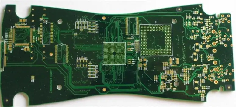
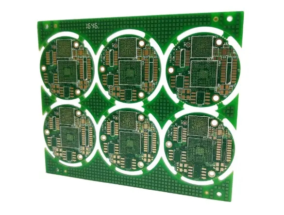
PCBA加工
Bad phenomena in PCBA processing and shielding interference sources in design
PCB manufacturers, PCB designers and PCBA manufacturers explain the undesirable phenomena that may occur in PCBA processing and the shielding interference sources in the design
During the processing and production of PCBA, some operational errors may lead to undesirable patch phenomena. What are the undesirable phenomena in PCBA processing?
1. Upright
Causes: uneven tension due to different sizes of copper and platinum on both sides; The heating rate of preheating is too fast; Machine mounting offset; Uneven solder paste printing thICkness; The temperature distribution in the reflow furnace is uneven; Solder paste printing offset; The clamping plate of the machine track is not tight, resulting in mounting offset, etc.
2. Short circuit
Causes: The space between the steel MESh and PCB board is too large, which causes the solder paste printing to be too thick, causing a short circuit; Short circuit caused by extrusion of solder paste due to low component mounting height; Short circuit caused by too fast temperature rise of the reflow furnace; Short circuit caused by component mounting offset; Poor steel mesh tapping (too thick, too long pin tapping, too large tapping) leads to short circuit, etc.
3. Offset
Cause: The positioning reference point on the circuit board is not clear; The positioning reference point on the circuit board is not aligned with the reference point on the screen board; The fixing and clamping of the circuit board in the printing machine are loose, and the positioning thimble is not in place.
4. Missing parts
Causes: Poor vacuum of the vacuum pump carbon chip, resulting in lack of parts; The suction nozzle is blocked or poor; Improper element thickness detection or poor detector; Improper setting of mounting height, etc.
5. Empty welding
Causes: weak activity of solder paste; Poor steel mesh opening; The spacing between copper and platinum is too large or the copper is pasted on SMAll components; Too much scraper pressure; Poor element pin flatness (warping, deformation), too fast temperature rise in preheating zone of back welding furnace, etc.
How to Shield the Propagation of Interference Sources in PCB design
Interference source refers to the element, equipment or signal generating interference; Propagation path refers to the path or medium through which interference propagates from the interference source to the sensitive device. What are the measures to cut off the interference propagation path in PCB design?
Fully consider the influence of power supply on MCU. If the power supply is well done, the anti-interference of the whole circuit will be more than half solved. Many single chip microcomputers are very sensitive to power supply noise. To reduce the interference of power supply noise on a single chip, filter circuits or voltage regulators should be added to the power supply of single chip microcomputers.
2. If the I/O port of the microcontroller is used to control noise devices such as motors, isolation shall be added between the I/O port and the noise source.
3. Pay attention to crystal oscillator wiring. The crystal oscillator shall be as close as possible to the pin of the microcontroller, and the clock area shall be isolated by the ground wire. The crystal oscillator shell shall be grounded and fixed.
4. The circuit board shall be zoned reasonably, and the interference sources (such as motors and relays) and sensitive components (such as single chip computers) shall be kept away as far as possible.
5. The digital area shall be isolated from the analog area with a ground wire. The digital ground shall be separated from the analog ground, and finally connected to the power supply ground at one point.
6. The ground wire of single chip microcomputer and high-power device shall be grounded separately to reduce mutual interference. High power devices shall be placed on the edge of the circuit board as far as possible.
7. Anti interference components, such as magnetic beads, magnetic rings, power filters, and shielding covers, are used in the I/O ports of single chip computers, power lines, circuit board connecting lines, and other key areas, which can significantly improve the anti-interference performance of the circuit.
PCB manufacturers, PCB designers and PCBA manufacturers explain the undesirable phenomena that may occur in PCBA processing and the shielding interference sources in the design.


抖音二維碼

Q Q二維碼

微信二維碼
點(diǎn)擊
然后
聯(lián)系
然后
聯(lián)系
電話熱線
13410863085Q Q

微信

- 郵箱