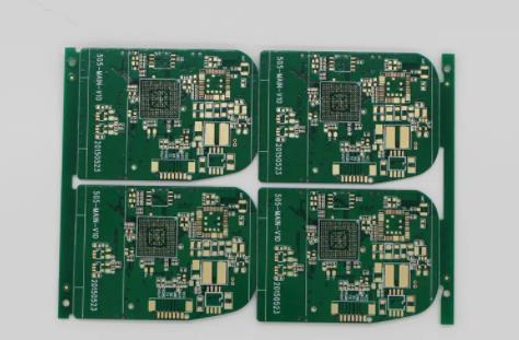
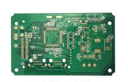
鑫景福致力于滿足“快速服務(wù),零缺陷,輔助研發(fā)”PCBA訂購單需求。


PCBA加工
Common Problems in the design of 66 PCB High Frequency Boards Part II
PCB manufacturers, PCB designers and PCBA manufacturers explain the common problems in the design of 66 PCB high-frequency boards Part II
With the rapid development of electronIC technology and the wide application of wireless communication technology in various fields, high-frequency, high-speed and high-density have gradually become one of the significant development trends of modern electronic products.
11. In the design of high-speed PCB, the blank area of the signal layer can be coated with copper, and how should the copper coating of multiple signal layers be distributed on the grounding and power supply?
Generally, the copper coating in the blank area is mostly grounded. It is only necessary to pay attention to the distance between the copper coating and the signal line when copper is applied beside the high-speed signal line, because the copper coating will reduce the characteristic impedance of the line. Also pay attention not to affect the characteristic impedance of other layers, such as in the structure of dual strip line.
12. Is it possible to use the microstrip line model to calculate the characteristic impedance of the signal line above the power plane? Can the signal between the power supply and the ground plane be calculated using the stripline model?
Yes, both the power plane and the ground plane must be considered as reference planes when calculating the characteristic impedance. For example, the four layer board: top layer - power layer - stratum - bottom layer. At this time, the model of the characteristic impedance of the top layer wiring is the microstrip line model with the power plane as the reference plane.

13. Can test points automatically generated by software on high-density printed boards meet the test requirements of mass production in general?
In general, whether the software automatically generates test points to meet the test requirements must depend on whether the specification of additional test points meets the requirements of the test equipment. In addition, if the routing is too dense and the specification for adding test points is strict, it may not be possible to automatically add test points to each segment of the line. Of course, you need to manually complete the place to be tested.
14. Will adding test points affect the quality of high-speed signals?
Whether it will affect the signal quality depends on the way of adding test points and how fast the signal is. Basically, the additional test points (not the online existing via or DIP pin as the test point) may be added to the online or pulLED out from the online for a short length of line.
The former is equivalent to adding a SMAll capacitor on line; The latter is an additional branch. Both of these two conditions will affect the high-speed signal more or less. The degree of influence is related to the frequency speed of the signal and the edge rate of the signal. The magnitude of the impact can be known through SIMulation. In principle, the smaller the test point, the better (and of course, meet the requirements of the test machine). The shorter the branch, the better.
15. Several PCBs constitute the system. How should the ground wires between the boards be connected?
When the signal or power supply between the interconnects of PCB boards acts, for example, if board A has power or the signal is sent to board B, there must be an equal amount of current flowing back from the stratum to board A (this is Kirchoff current law). The current in this stratum will flow back to the place with the lowest impedance. Therefore, the number of pins allocated to the formation at each interface, whether the power supply or signal is connected, cannot be too small to reduce impedance, which can reduce the noise on the formation.
In addition, it is also possible to analyze the entire current loop, especially the part with large current, and adjust the grounding method of the stratum or ground wire to control the current path (for example, make a low impedance at a certain place to let most of the current flow from this place), so as to reduce the impact on other sensitive signals.
16. Can you introduce some foreign technical books and data on high-speed PCB design?
Nowadays, high-speed digital circuits are used in communication networks, calculators and other related fields. In terms of communication network, the working frequency of PCB board has reached GHz, and the number of layers is up to 40 as far as I know. Due to the progress of the chip, the highest working frequency on the board of a general PC or server has reached more than 400MHz (such as Rambus). In response to the demand for high-speed and high-density routing, the demand for blind/buried vias, mirrovias and build up processes is also increasing. These design requirements can be mass produced by manufacturers.
17. Two frequently referenced characteristic impedance formulas
microstrip Z={87/[sqrt (Er+1.41)]} ln [5.98H/(0.8W+T)], where W is the line width, T is the copper sheet thickness of the routing, H is the distance from the routing to the reference plane, and Er is the dielectric constant of the PCB material. This formula can only be applied when 0.1<(W/H)<2.0 and 1<(Er)<15.
stripline Z=[60/sqrt (Er)] ln {4H/[0.67 π (T+0.8W)]}, where H is the distance between two reference planes, and the routing is in the middle of the two reference planes. This formula can only be applied when W/H<0.35 and T/H<0.25.
18. Can a ground wire be added in the middle of the differential signal line?
Generally, the differential signal cannot be grounded. Because the most important point of differential signal application principle is to use the benefits of coupling between differential signals, such as flux cancellation, noise immunity, etc. If a ground wire is added in the middle, the coupling effect will be destroyed.
19. Does rigid flexible plate design require special design software and specifications? Where can we undertake such PCB processing in China?
Flexible printed circuit can be designed with general PCB design software. It is also produced by FPC manufacturers in Gerber format. Since the manufacturing process is different from that of general PCBs, each manufacturer will limit the minimum line width, minimum line spacing and minimum aperture (via) according to their manufacturing capacity.
In addition, copper sheet can be laid at the turning point of the Flexible circuit board for reinforcement. As for the manufacturer, it can be found by using "FPC" as the keyword query.
20. What is the principle of properly selecting the grounding point between PCB and housing?
The principle of selecting PCB and housing grounding point is to use the chassis ground to provide a low impedance path to the return current and control the path of the return current. For example, it is usually possible to connect the PCB layer with the chassis ground near the high-frequency device or clock generator by using the fixing screws to minimize the area of the entire current loop, and thus reduce electromagnetic radiation. PCB manufacturers, PCB designers, and PCBA manufacturers will explain the second part of the common problems in the design of 66 PCB high-frequency boards.


抖音二維碼

Q Q二維碼

微信二維碼
點擊
然后
聯(lián)系
然后
聯(lián)系
電話熱線
13410863085Q Q

微信

- 郵箱