鑫景福致力于滿足“快速服務,零缺陷,輔助研發”PCBA訂購單需求。


PCBA加工

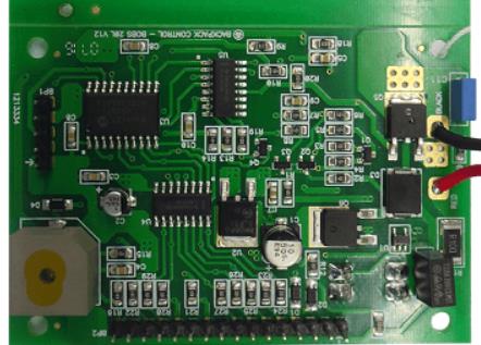
surface mounting and devICe cracking in PCBA processing
In PCBA processing, the most commonly used installation technology is SMT wafer processing technology SMT wafer processing is a circuit assembly technology that attaches and solders surface mount components to a specified position on the surface of a printed circuit board It is widely used in large circuit board manufacturers and is the most popular technology and process at present
1. Reasons for using PCBA to treat SMT:
1. The electronic products are pursuing miniaturization, and the previously used perforated plug-in components can no longer be reduced;
2. The functions of electronic products are more complete. The integrated circuit (IC) used does not have perforated components, especially for large-scale and highly integrated IC, and surface mount components must be used;
3. Mass production and production automation. The factory must produce high-quality products with low cost and high output to meet customer needs and enhance MARKet competitiveness;
2. Advantages of SMT chip processing:
1. High reliability, strong anti vibration ability, low solder joint defect rate;
2. Good high frequency characteristics, reduce electromagnetic and radio frequency interference;
3. Electronic products have high assembly density, SMAll volume and light weight. The volume and weight of SMT components are only about 1/10 of those of traditional components. Generally speaking, the volume of electronic products has been reduced by 40% - 60% and the weight has been reduced by 60% - 80% after the use of Surface Mount Technology;
4. It is easy to realize automation, improve production efficiency, reduce costs by 30% - 50%, and save data, energy, equipment, manpower, time, etc.
3. Scientific and technological components related to SMT chip processing:
1. design and manufacturing technology of electronic components and integrated circuits;
2. circuit design technology of electronic products;
3. Manufacturing technology of circuit board;
4. Design and manufacturing technology of automatic placement equipment;
5. Technology of circuit component manufacturing;
6. Development and production technology of auxiliary materials for assembly and manufacturing.
Solution for cracking SMT chip processing equipment
Reasons for Cracking of SMT Wafer Processing Equipment
1. As for MLCC capacitor, its structure is composed of multilayer ceramic capacitors. In addition, its structure is weak, strength is low, heat resistance is strong and mechanical impact is strong, which is especially obvious in wave soldering.
2. During SMT placement, the suction and release height of the Z-axis of the placement machine, especially for some placement machines that do not have the Z-axis soft landing function, depends on the thickness of the chip assembly, not through the pressure sensor. The tolerance of the thickness of this assembly may cause cracks.
3. After welding, if there is warping stress on PCB, it is easy to cause component cracking.
4. PCB stresses during splicing can also damage components.
Mechanical stress during ICT testing resulted in equipment breakage.
Stress during assembly can damage the MLCC around the fastening screws.
Solution to SMT chip processing equipment
1. Carefully adjust the welding process curve, especially the heating speed should not be too fast.
2. During the placement, please ensure that the machine pressure is correctly placed, especially for thick plates and metal substrates, as well as ceramic substrates used for installing MLCC and other brittle equipment.
3. Pay attention to the placement method and shape of the tool
4. The warpage of PCB, especially after welding, shall be specially corrected to prevent the stress caused by large deformation from affecting the device.
5. During this period, PCB is designed to avoid high stress areas of MLCC and other equipment
In PCBA processing, the most commonly used installation technology is SMT wafer processing technology SMT wafer processing is a circuit assembly technology that attaches and solders surface mount components to a specified position on the surface of a printed circuit board It is widely used in large circuit board manufacturers and is the most popular technology and process at present
1. Reasons for using PCBA to treat SMT:
1. The electronic products are pursuing miniaturization, and the previously used perforated plug-in components can no longer be reduced;
2. The functions of electronic products are more complete. The integrated circuit (IC) used does not have perforated components, especially for large-scale and highly integrated IC, and surface mount components must be used;
3. Mass production and production automation. The factory must produce high-quality products with low cost and high output to meet customer needs and enhance MARKet competitiveness;

2. Advantages of SMT chip processing:
1. High reliability, strong anti vibration ability, low solder joint defect rate;
2. Good high frequency characteristics, reduce electromagnetic and radio frequency interference;
3. Electronic products have high assembly density, SMAll volume and light weight. The volume and weight of SMT components are only about 1/10 of those of traditional components. Generally speaking, the volume of electronic products has been reduced by 40% - 60% and the weight has been reduced by 60% - 80% after the use of Surface Mount Technology;
4. It is easy to realize automation, improve production efficiency, reduce costs by 30% - 50%, and save data, energy, equipment, manpower, time, etc.
3. Scientific and technological components related to SMT chip processing:
1. design and manufacturing technology of electronic components and integrated circuits;
2. circuit design technology of electronic products;
3. Manufacturing technology of circuit board;
4. Design and manufacturing technology of automatic placement equipment;
5. Technology of circuit component manufacturing;
6. Development and production technology of auxiliary materials for assembly and manufacturing.
Solution for cracking SMT chip processing equipment
Reasons for Cracking of SMT Wafer Processing Equipment
1. As for MLCC capacitor, its structure is composed of multilayer ceramic capacitors. In addition, its structure is weak, strength is low, heat resistance is strong and mechanical impact is strong, which is especially obvious in wave soldering.
2. During SMT placement, the suction and release height of the Z-axis of the placement machine, especially for some placement machines that do not have the Z-axis soft landing function, depends on the thickness of the chip assembly, not through the pressure sensor. The tolerance of the thickness of this assembly may cause cracks.
3. After welding, if there is warping stress on PCB, it is easy to cause component cracking.
4. PCB stresses during splicing can also damage components.
Mechanical stress during ICT testing resulted in equipment breakage.
Stress during assembly can damage the MLCC around the fastening screws.
Solution to SMT chip processing equipment
1. Carefully adjust the welding process curve, especially the heating speed should not be too fast.
2. During the placement, please ensure that the machine pressure is correctly placed, especially for thick plates and metal substrates, as well as ceramic substrates used for installing MLCC and other brittle equipment.
3. Pay attention to the placement method and shape of the tool
4. The warpage of PCB, especially after welding, shall be specially corrected to prevent the stress caused by large deformation from affecting the device.
5. During this period, PCB is designed to avoid high stress areas of MLCC and other equipment


抖音二維碼

Q Q二維碼

微信二維碼
點擊
然后
聯系
然后
聯系
電話熱線
13410863085Q Q

微信

- 郵箱