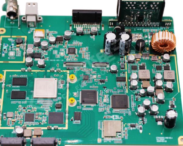
鑫景福致力于滿足“快速服務(wù),零缺陷,輔助研發(fā)”PCBA訂購單需求。


PCBA加工
SMT solder, wave crest and cooling wave crest
SMT assembly process is closely related to each process step before welding, including capital investment, PCB design, component solderability, assembly operation, flux selection, temperature/time control, solder and crystal structure, etc
1 PCB solder
At present, the most commonly used solder for wave soldering is eutectIC tin lead alloy: tin 63%; Lead 37%. The temperature of solder in the solder pot shall be maintained at all tiMES, and the temperature shall be higher than the alloy liquid temperature of 183 ℃, and the temperature shall be uniform. In the past, a solder pot temperature of 250 ° C was considered "standard".
With the innovation of flux technology, the uniformity of solder temperature in the entire solder pot is controlLED, and a preheater is added. The development trend is to use temperature
The solder composition in the solder pot is closely related to time, that is, it changes with time, which leads to the formation of scum. This is why welding parts and residues and other metal impurities in the welding process should be removed. Causes of tin loss. These factors will reduce the fluidity of solder. During the procurement process, the maximum content of tin in metal micro dross and solder must be specified in various standards (for example, IPC/J-STD-006 has clear provisions). During welding, ANSI/J-STD-001B standard also specifies the requirements for solder purity. 63% tin except restricted scum; 37% lead alloys require tin content not less than 61.5%. The concentration of gold and copper in the organic bath layer on wave soldering components accumulates faster than in the past. This accumulation, coupled with significant tin loss, can cause loss of solder flow and lead to welding problems. Rough, granular solder joints are usually caused by dross in solder. Dim and rough granular solder joints formed by dross accumulated in the solder pot or inherent residues of the component itself may also be a sign of low tin content. This is not the result of tin loss in local special solder joints or tin pots. This appearance may also be caused by vibration or impact during solidification.
The appearance of solder joints can directly reflect the process or data problems. To maintain the "full pot" state of solder, and check the solder according to the process control plan
Pot analysis is very important. As there is scum in the solder can, it is usually unnecessary to "pour out" the flux in the solder can. In traditional applications, it is necessary to add solder to the solder pot so that the solder in the pot is always full. In the case of tin loss, the addition of pure tin helps to maintain the desired concentration. In order to monitor the compounds in the tin cans, a routine analysis should be performed. If tin is added, the sample shall be sampled and analyzed to ensure the correct solder composition ratio. Excessive scum is another thorny problem. There is no doubt that scum is always present in the solder pot, especially when welding in the atmOSPhere. The use of "wafer wave crest" is very helpful for welding high-density components, because the solder surface exposed to the atmosphere is too large, and the solder will be oxidized, which will produce more scum. The solder surface in the solder pot is covered by the scum layer, and the oxidation rate is slowed down.
During the welding process, more scum will be produced due to the turbulence and flow of the wave crest in the tin can. The recommended traditional method is skimming. If the slag is skimmed frequently, more scum will be produced and more solder will be consumed. The scum may also be mixed in the wave crest, causing the wave crest to be unstable or turbulent. This requires more maintenance of the liquid composition in the solder pot. If it is allowed to reduce the amount of solder in the tin can, the dross on the solder surface will enter the pump, which is likely to occur. Sometimes, granular solder joints are mixed with dross. The scum found initially may be caused by rough peaks and may block the pump. The tin can shall be equipped with adjustable low capacity solder sensor and alarm device.
2 crests
In the process of wave soldering, wave crest is the core. Preheating, flux coating and uncontaminated metal can be sent to the welding station through the conveyor belt for contact
Then, the solder with a certain temperature is heated to make the solder react chEMIcally, and the solder alloy will form interconnection through wave power. This is the most critical step. At present, the commonly used symmetrical peak is called the main peak. Set the pump speed, wave crest height, penetration depth, transmission angle and transmission rate to provide all-round conditions for achieving good welding characteristics. The PCB data shall be adjusted properly. After the solder leaves the top (outlet end), the speed shall be slowed down and the operation shall be stopped slowly. When the waveform runs, the PCB will eventually push the solder to the outlet. Under the most overhanging conditions, the solder surface tension and optimized circuit board peak operation can achieve zero relative movement between the component and the outlet wave peak. The shelling area is used to remove solder from the circuit board. Sufficient inclination angle shall be provided to avoid defects such as bridging, burr, wire drawing and welding ball. Sometimes, hot air flow is required at the crest outlet to ensure that possible bridges are eliminated. After surface mount components are installed at the bottom of the board, sometimes turbulence wafer wave peaks are used before the wave peaks are leveled to compensate for the flux or bubbles in the "rough wave peak" area formed later. The high vertical velocity of the turbulence wave crest helps to ensure that the solder is in contact with the lead or pad. The vibrating part behind the flat laminar wave crest can also be used to eliminate bubbles and ensure satisfactory contact between solder and parts. The welding station shall basically: high-purity solder (according to the standard), peak temperature (230 250 ℃), total contact time (35 seconds), and immersion depth of the printed board into the wave crest (50 80%), so as to realize the parallel transmission path when the wave crest is parallel to the rail and the flux content in the tin bath.
3 Wave post weld cooling
The cooling station is usually added to the tail of the wave soldering machine. In order to limit the tendency of copper tin intermetallic compounds to form solder joints, another reason is to accelerate
When the solder is not completely cured, component cooling can prevent the circuit board from moving Cool the components quickly to limit the exposure of sensitive components to high temperatures However, the damage of thermal shock of aggressive cooling system to components and solder joints shall be considered The forced air cooling system shall not damage the most serious PCB components due to the "soft and stable" of good control. There are two reasons for using this system: it can quickly process the circuit board without manually holding the circuit board, and it can ensure that the temperature of the components is lower than that of the cleaning solution People are concerned about the latter reason, which may be the cause of foaming of some flux residues Another phenomenon is that it sometimes reacts with some flux scum, so the residue is "non cleanable" Ensure that the data set of the welding workstation meets the requirements of all machines, all PCB designs, all data used, and the data conditions and requirements of PCB processes. No formula can meet these requirements You must understand each step of the whole PCB process
SMT assembly process is closely related to each process step before welding, including capital investment, PCB design, component solderability, assembly operation, flux selection, temperature/time control, solder and crystal structure, etc
1 PCB solder
At present, the most commonly used solder for wave soldering is eutectIC tin lead alloy: tin 63%; Lead 37%. The temperature of solder in the solder pot shall be maintained at all tiMES, and the temperature shall be higher than the alloy liquid temperature of 183 ℃, and the temperature shall be uniform. In the past, a solder pot temperature of 250 ° C was considered "standard".
With the innovation of flux technology, the uniformity of solder temperature in the entire solder pot is controlLED, and a preheater is added. The development trend is to use temperature

The solder composition in the solder pot is closely related to time, that is, it changes with time, which leads to the formation of scum. This is why welding parts and residues and other metal impurities in the welding process should be removed. Causes of tin loss. These factors will reduce the fluidity of solder. During the procurement process, the maximum content of tin in metal micro dross and solder must be specified in various standards (for example, IPC/J-STD-006 has clear provisions). During welding, ANSI/J-STD-001B standard also specifies the requirements for solder purity. 63% tin except restricted scum; 37% lead alloys require tin content not less than 61.5%. The concentration of gold and copper in the organic bath layer on wave soldering components accumulates faster than in the past. This accumulation, coupled with significant tin loss, can cause loss of solder flow and lead to welding problems. Rough, granular solder joints are usually caused by dross in solder. Dim and rough granular solder joints formed by dross accumulated in the solder pot or inherent residues of the component itself may also be a sign of low tin content. This is not the result of tin loss in local special solder joints or tin pots. This appearance may also be caused by vibration or impact during solidification.
The appearance of solder joints can directly reflect the process or data problems. To maintain the "full pot" state of solder, and check the solder according to the process control plan
Pot analysis is very important. As there is scum in the solder can, it is usually unnecessary to "pour out" the flux in the solder can. In traditional applications, it is necessary to add solder to the solder pot so that the solder in the pot is always full. In the case of tin loss, the addition of pure tin helps to maintain the desired concentration. In order to monitor the compounds in the tin cans, a routine analysis should be performed. If tin is added, the sample shall be sampled and analyzed to ensure the correct solder composition ratio. Excessive scum is another thorny problem. There is no doubt that scum is always present in the solder pot, especially when welding in the atmOSPhere. The use of "wafer wave crest" is very helpful for welding high-density components, because the solder surface exposed to the atmosphere is too large, and the solder will be oxidized, which will produce more scum. The solder surface in the solder pot is covered by the scum layer, and the oxidation rate is slowed down.
During the welding process, more scum will be produced due to the turbulence and flow of the wave crest in the tin can. The recommended traditional method is skimming. If the slag is skimmed frequently, more scum will be produced and more solder will be consumed. The scum may also be mixed in the wave crest, causing the wave crest to be unstable or turbulent. This requires more maintenance of the liquid composition in the solder pot. If it is allowed to reduce the amount of solder in the tin can, the dross on the solder surface will enter the pump, which is likely to occur. Sometimes, granular solder joints are mixed with dross. The scum found initially may be caused by rough peaks and may block the pump. The tin can shall be equipped with adjustable low capacity solder sensor and alarm device.
2 crests
In the process of wave soldering, wave crest is the core. Preheating, flux coating and uncontaminated metal can be sent to the welding station through the conveyor belt for contact
Then, the solder with a certain temperature is heated to make the solder react chEMIcally, and the solder alloy will form interconnection through wave power. This is the most critical step. At present, the commonly used symmetrical peak is called the main peak. Set the pump speed, wave crest height, penetration depth, transmission angle and transmission rate to provide all-round conditions for achieving good welding characteristics. The PCB data shall be adjusted properly. After the solder leaves the top (outlet end), the speed shall be slowed down and the operation shall be stopped slowly. When the waveform runs, the PCB will eventually push the solder to the outlet. Under the most overhanging conditions, the solder surface tension and optimized circuit board peak operation can achieve zero relative movement between the component and the outlet wave peak. The shelling area is used to remove solder from the circuit board. Sufficient inclination angle shall be provided to avoid defects such as bridging, burr, wire drawing and welding ball. Sometimes, hot air flow is required at the crest outlet to ensure that possible bridges are eliminated. After surface mount components are installed at the bottom of the board, sometimes turbulence wafer wave peaks are used before the wave peaks are leveled to compensate for the flux or bubbles in the "rough wave peak" area formed later. The high vertical velocity of the turbulence wave crest helps to ensure that the solder is in contact with the lead or pad. The vibrating part behind the flat laminar wave crest can also be used to eliminate bubbles and ensure satisfactory contact between solder and parts. The welding station shall basically: high-purity solder (according to the standard), peak temperature (230 250 ℃), total contact time (35 seconds), and immersion depth of the printed board into the wave crest (50 80%), so as to realize the parallel transmission path when the wave crest is parallel to the rail and the flux content in the tin bath.
3 Wave post weld cooling
The cooling station is usually added to the tail of the wave soldering machine. In order to limit the tendency of copper tin intermetallic compounds to form solder joints, another reason is to accelerate
When the solder is not completely cured, component cooling can prevent the circuit board from moving Cool the components quickly to limit the exposure of sensitive components to high temperatures However, the damage of thermal shock of aggressive cooling system to components and solder joints shall be considered The forced air cooling system shall not damage the most serious PCB components due to the "soft and stable" of good control. There are two reasons for using this system: it can quickly process the circuit board without manually holding the circuit board, and it can ensure that the temperature of the components is lower than that of the cleaning solution People are concerned about the latter reason, which may be the cause of foaming of some flux residues Another phenomenon is that it sometimes reacts with some flux scum, so the residue is "non cleanable" Ensure that the data set of the welding workstation meets the requirements of all machines, all PCB designs, all data used, and the data conditions and requirements of PCB processes. No formula can meet these requirements You must understand each step of the whole PCB process


抖音二維碼

Q Q二維碼

微信二維碼
點(diǎn)擊
然后
聯(lián)系
然后
聯(lián)系
電話熱線
13410863085Q Q

微信

- 郵箱