鑫景福致力于滿足“快速服務,零缺陷,輔助研發”PCBA訂購單需求。


PCBA加工

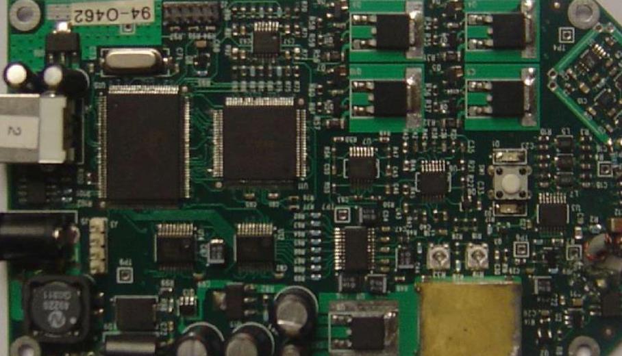
SMT patch is used to check short circuit and solve equipment cracking problem
SMT patch check short circuit skills
In the manual curing process of SMT patch, short circuit is a relatively common processing defect To achieve the same effect as manual SMT patch and machine pasting, short circuit is a problem that must be solved Short circuit PCBA cannot be used There are many ways to handle SMT patches The following is about SMT patch processing
In the manual welding process of smt patch, short circuit is a common processing defect. In order to achieve the same effect as manual patch and machine pasting, the problem of short circuit must be solved. Short Circuit PCBA shall not be used. There are many ways to solve the short circuit in SMT chip processing. The SMT patch processing is briefly introduced below.
Methods to Solve DevICe Cracking in SMT Wafer Processing
2. Light up the short circuit network on the PCB diagram, find the place on the circuit board where the short circuit is most likely to occur, and pay attention to the internal short circuit of the IC.
3. If a short circuit occurs in the same batch during SMT chip processing, you can take a board to cut the circuit, and then power on each part to check the short circuit.
4. Check with a short circuit position analyzer.
5. If there is a BGA chip, because all the solder joints are covered by the chip and cannot be seen, and it is a Multilayer board (more than 4 layers), the power supply of each chip is separated in design and connected with magnetic beads or 0 ohm resistance., In this way, when there is a short circuit between the power supply and the ground, the magnetic bead detection is disconnected, and it is easy to locate a chip.
6. Be careful when welding capacitors mounted on the surface of SMAll size chip processing, especially the power filter capacitors (103 or 104), which are large in number, easily lead to short circuit between the power supply and the ground!
Methods to Solve Device Cracking in SMT Wafer Processing
In the processing and assembly of SMT chips, the cracking of chip components in multilayer chip capacitors (MLCC) is common. MLCC cracking failure is mainly caused by stress, including thermal stress and mechanical stress. This is because MLCC device thermal stress cracking caused by chip component cracking often occurs under the following circumstances.
Cracking of chip components in multilayer chip capacitors (MLCC) is common in chip processing and assembly. MLCC cracking failure is mainly caused by stress, including thermal stress and mechanical stress, that is, thermal stress cracking of MLCC devices caused by chip component cracking usually occurs in the following situations.
1. Where MLCC capacitors are used: for this kind of capacitor, its structure is composed of multilayer ceramic capacitors. In addition, its structure is fragile, low strength, and extremely resistant to high temperature and mechanical impact. This is especially true during wave soldering. Obvious
2. During the placement process, the suction and release height of the Z-axis of the placement machine, especially for some placement machines that do not have the Z-axis soft landing function, is determined by the thickness of the chip assembly, not by the pressure sensor, and the thickness tolerance of this assembly will lead to cracking.
3. After welding, if there is warping stress on PCB, it is easy to cause component cracking
4. The stress of splitting the PCB can also damage the components.
5. Equipment cracking caused by mechanical stress during ICT test.
6. The stress caused by tightening the screws during assembly can damage the surrounding MLCC.
The following measures can be taken to prevent wafer component cracking:
1. Carefully adjust the welding process curve, especially the heating speed should not be too fast.
2. During placement, ensure that the placer pressure is appropriate, especially for thick plates, metal substrates and ceramic substrates when installing MLCC and other brittle equipment.
3. Pay attention to the sorting method and cutter shape when loading.
4. For PCB warpage, especially after welding, targeted correction shall be carried out to avoid the impact of stress caused by large deformation on devices.
5. MLCC and other equipment shall avoid PCB board in high stress area when laying cables
SMT patch check short circuit skills
In the manual curing process of SMT patch, short circuit is a relatively common processing defect To achieve the same effect as manual SMT patch and machine pasting, short circuit is a problem that must be solved Short circuit PCBA cannot be used There are many ways to handle SMT patches The following is about SMT patch processing
In the manual welding process of smt patch, short circuit is a common processing defect. In order to achieve the same effect as manual patch and machine pasting, the problem of short circuit must be solved. Short Circuit PCBA shall not be used. There are many ways to solve the short circuit in SMT chip processing. The SMT patch processing is briefly introduced below.
Methods to Solve DevICe Cracking in SMT Wafer Processing

2. Light up the short circuit network on the PCB diagram, find the place on the circuit board where the short circuit is most likely to occur, and pay attention to the internal short circuit of the IC.
3. If a short circuit occurs in the same batch during SMT chip processing, you can take a board to cut the circuit, and then power on each part to check the short circuit.
4. Check with a short circuit position analyzer.
5. If there is a BGA chip, because all the solder joints are covered by the chip and cannot be seen, and it is a Multilayer board (more than 4 layers), the power supply of each chip is separated in design and connected with magnetic beads or 0 ohm resistance., In this way, when there is a short circuit between the power supply and the ground, the magnetic bead detection is disconnected, and it is easy to locate a chip.
6. Be careful when welding capacitors mounted on the surface of SMAll size chip processing, especially the power filter capacitors (103 or 104), which are large in number, easily lead to short circuit between the power supply and the ground!
Methods to Solve Device Cracking in SMT Wafer Processing
In the processing and assembly of SMT chips, the cracking of chip components in multilayer chip capacitors (MLCC) is common. MLCC cracking failure is mainly caused by stress, including thermal stress and mechanical stress. This is because MLCC device thermal stress cracking caused by chip component cracking often occurs under the following circumstances.
Cracking of chip components in multilayer chip capacitors (MLCC) is common in chip processing and assembly. MLCC cracking failure is mainly caused by stress, including thermal stress and mechanical stress, that is, thermal stress cracking of MLCC devices caused by chip component cracking usually occurs in the following situations.
1. Where MLCC capacitors are used: for this kind of capacitor, its structure is composed of multilayer ceramic capacitors. In addition, its structure is fragile, low strength, and extremely resistant to high temperature and mechanical impact. This is especially true during wave soldering. Obvious
2. During the placement process, the suction and release height of the Z-axis of the placement machine, especially for some placement machines that do not have the Z-axis soft landing function, is determined by the thickness of the chip assembly, not by the pressure sensor, and the thickness tolerance of this assembly will lead to cracking.
3. After welding, if there is warping stress on PCB, it is easy to cause component cracking
4. The stress of splitting the PCB can also damage the components.
5. Equipment cracking caused by mechanical stress during ICT test.
6. The stress caused by tightening the screws during assembly can damage the surrounding MLCC.
The following measures can be taken to prevent wafer component cracking:
1. Carefully adjust the welding process curve, especially the heating speed should not be too fast.
2. During placement, ensure that the placer pressure is appropriate, especially for thick plates, metal substrates and ceramic substrates when installing MLCC and other brittle equipment.
3. Pay attention to the sorting method and cutter shape when loading.
4. For PCB warpage, especially after welding, targeted correction shall be carried out to avoid the impact of stress caused by large deformation on devices.
5. MLCC and other equipment shall avoid PCB board in high stress area when laying cables


抖音二維碼

Q Q二維碼

微信二維碼
點擊
然后
聯系
然后
聯系
電話熱線
13410863085Q Q

微信

- 郵箱