鑫景福致力于滿足“快速服務,零缺陷,輔助研發”PCBA訂購單需求。


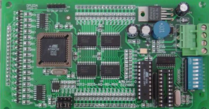
PCBA加工
Six BasIC Principles of SMB design
SMB Design
1. Layout of components
The layout is to arrange the components evenly and orderly on the PCB according to the requirements of the electrical schematic diagram and the size of the components, and can meet the mechanical and electrical efficiency requirements of the whole machine Whether the layout is reasonable not only affects the efficiency and reliability of the system PCB components and the whole machine, but also affects the difficulty of PCB and its assembly, processing and maintenance. Therefore, please try to perform the following operations during the layout:
The components shall be evenly distributed, and the components of the same unit circuit shall be relatively centralized for debugging and maintenance;
Components with interconnection shall be arranged relatively close to each other to increase wiring density and ensure the shortest wiring distance;
Heat sensitive parts shall be far away from parts that generate a lot of heat;
Components that may have electromagnetic interference with each other shall be shielded or isolated.
2. Wiring rules
Wiring is to arrange printed wires according to electrical schematic diagram, wire list and required wire width and spacing. Wiring shall generally comply with the following rules:
On the prEMIse of meeting the use requirements, the wiring can be SIMple but not complex, and the sequence of wiring methods is single-layer, double-layer and multi-layer.
The wire layout between two connecting boards shall be as short as possible, and sensitive signals and SMAll signals shall be given priority to reduce the delay and interference of small signals. Ground wire shield shall be laid near the input line of analog circuit; Wiring on the same layer shall be evenly distributed; The conductive area on each layer shall be relatively balanced to prevent the circuit board from warping.
When changing the direction of signal line, it shall be inclined or smooth, and the radius of curvature shall be large to avoid electric field concentration, signal reflection and additional impedance.
circuit board
The wiring of digital circuit and analog circuit shall be separated to avoid mutual interference. If they are on the same layer, the conductors of the grounding system and power supply system of the two circuits shall be laid separately, and the signal wires of different frequencies shall be separated by laying ground wires., Avoid crosstalk. In order to facilitate testing, necessary breakpoints and test points shall be set in the design.
When the circuit element is grounded and connected to the power supply, the trace should be as short as possible and as close as possible to reduce internal resistance.
The upper and lower traces should be perpendicular to each other to reduce coupling, and the upper and lower traces should not be aligned or parallel.
Multiple input/output lines of high-speed circuit and input/output lines of circuit (such as differential amplifier and balanced amplifier) shall be of equal length to avoid unnecessary delay or phase shift.
When the bonding pad is connected to a large conductive area, thin wires with a length of not less than 0.5mm shall be used for heat insulation, and the width of the thin wire shall not be less than 0.13mm.
The wire closest to the edge of the circuit board shall be more than 5mm away from the edge of the circuit board. If necessary, the grounding wire can be close to the edge of the circuit board. If the guide rail is to be inserted during PCB processing, the distance between the wire and the edge of the PCB must be at least greater than the depth of the guide rail slot.
The public power cord and ground wire on the double-sided board shall be as close to the edge of the board as possible and distributed on the surface of the board. The Multilayer board can be provided with a power layer and a ground layer in the inner layer, and connected to the power lines and ground wires of each layer through the metallization holes. Adhesion between layers of multilayer board.
3. Conductor width
The width of the printed wire is determined by the load current of the wire, the allowable temperature rise and the adhesion of the copper foil. Generally, the line width of the printed board is not less than 0.2mm and the thickness is greater than 18mm. The thinner the wire, the more difficult it is to process. In this case, when the wiring space is allowed, the wider conductor shall be selected appropriately. The general design principles are as follows:
The thickness of signal lines should be the same, which is conducive to impedance matching. Generally, the recommended line width is 0.2~0.3mm (812mil). For the power grounding wire, the larger the connection area, the less interference. It is better to mask high-frequency signals with ground wires, which can improve the transmission effect.
In high-speed circuit and microwave circuit, the characteristic impedance of transmission line is specified. At this time, the width and thickness of the conductor shall meet the requirements of characteristic impedance.
When designing high power circuits, power density should also be considered. In this case, the line width, thickness and insulation efficiency between lines shall be considered. If it is an inner conductor, the allowable current density is about half of the outer conductor.
4. Printed wire spacing
The insulation resistance between the conductors on the surface of the printed board is determined by the conductor spacing, the length of the parallel section of adjacent conductors and the insulation medium (including the substrate and air). When the wiring space is allowed, the spacing of conductors shall be increased appropriately.
5. Selection of components
PCB board shall be fully considered in the selection of components, and traditional components shall be used as far as possible Do not blindly pursue small size components to avoid new costs Attention shall be paid to the pin shape and pin spacing of integrated circuit devices QFP with pin spacing less than 0 should be carefully considered for 5mm It is better to choose BGA packaging equipment directly In addition, temperature tolerance (such as which it can meet the needs of lead free soldering) should be considered
After part selection, a part database must be established, including relevant information such as installation size, pin size and manufacturer.
6. Selection of PCB base plate
The substrate should be selected according to the use conditions and mechanical and electrical performance requirements of the PCB; the number of copper-clad surfaces of the substrate (single-sided, double-sided or multi-layer board) should be determined according to the printed board structure; according to the size of the printed board, the tissue area bears the quality of the components and determines the thickness of the substrate The cost of different types of data varies greatly The following factors shall be considered when selecting: PCB base plate
Power efficiency requirements;
Thermogravimetry, coefficient of thermal expansion, flatness and pore metallization ability;
Price factor.
Six Common Integrated Circuit Packages
12-03,2022


抖音二維碼

Q Q二維碼

微信二維碼
點擊
然后
聯系
然后
聯系
電話熱線
13410863085Q Q

微信

- 郵箱