鑫景福致力于滿足“快速服務(wù),零缺陷,輔助研發(fā)”PCBA訂購單需求。


PCBA加工

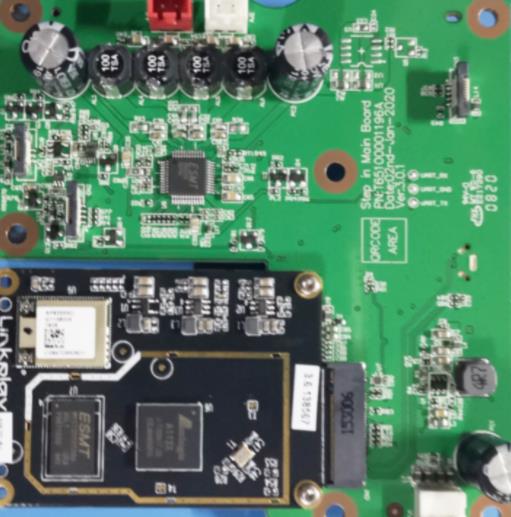
Introduce the production process of SMT chip PCB
It is very important to partICipate in PCB manufacturing process in electronic industry printed circuit board, printed circuit board, is widely used as the basis of electronic circuits printed circuit boards are used to provide a mechanical basis on which circuits can be built In retrOSPect, almost all printed circuit boards and their designs used for circuits are used by millions of people
Although today's PCBs form the basis of almost all electronic circuits, they are usually taken for granted However, science and technology in this area are progressing The track size is reduced, the number of layers is being added to adapt to the new connections required, and the design rules are being improved to ensure that SMAller SMT equipment can handle and adapt to the welding process used in production
The PCB manufacturing process can be implemented in many ways and has many variations. Although there are many small changes, the main stages in the PCB manufacturing process are the same.
PCB composition
In order to form a track with the components in the PCB, the copper clad plate is first obtained. This includes both sides of the substrate material (usually FR4) and the usual copper cladding. The copper coating is attached to a thin layer of copper on the motherboard. This combination is usually very beneficial to FR4, but the characteristics of PTFE make it more difficult, which increases the difficulty of PTFE PCB processing.
Basic PCB manufacturing technology
After selecting and providing the bare PCB, the next step is to create the desired tracks on the PCB and remove the unwanted copper. PCB is usually manufactured by chEMIcal etching process. The most common PCB etching form is ferric chloride.
In order to obtain the correct track pattern, the photography process is used. Generally, the copper of bare PCB is covered with a thin layer of photoresist. It then specifies the desired trace exposure through photographic film or a mask. Through this pipe, the image of the track is transferred to the photoresist. After completion, the photoresist is placed in the developer so that only the required track plate area is covered with the photoresist.
The next stage of the process is to place the printed circuit board in the ferric chloride etching area, which does not require rails or copper. After knowing the concentration of FeCl3 and the thickness of copper on the circuit board, put it into the amount of time required for etching bubble e-commerce. If the printed circuit board is placed in the etching for too long, some clarity will be lost, because the 3 ferric chloride will weaken the photoresist.
Although most PCB boards are made by photographic processing, other methods can also be used. One is to use professional high-precision milling machine. Then control the machine to grind the copper to a far place where it is not needed. The control is obviously automatic, driven by files generated by PCB design software. This form of PCB manufacturing is not suitable for mass production, but it is an ideal choice in many cases where a very small number of PCB prototypes are required.
The other is sometiMES used for PCB Prototype is to print an etching resist ink on the printed circuit board using the screen printing process
It is very important to partICipate in PCB manufacturing process in electronic industry printed circuit board, printed circuit board, is widely used as the basis of electronic circuits printed circuit boards are used to provide a mechanical basis on which circuits can be built In retrOSPect, almost all printed circuit boards and their designs used for circuits are used by millions of people
Although today's PCBs form the basis of almost all electronic circuits, they are usually taken for granted However, science and technology in this area are progressing The track size is reduced, the number of layers is being added to adapt to the new connections required, and the design rules are being improved to ensure that SMAller SMT equipment can handle and adapt to the welding process used in production
The PCB manufacturing process can be implemented in many ways and has many variations. Although there are many small changes, the main stages in the PCB manufacturing process are the same.
PCB composition

In order to form a track with the components in the PCB, the copper clad plate is first obtained. This includes both sides of the substrate material (usually FR4) and the usual copper cladding. The copper coating is attached to a thin layer of copper on the motherboard. This combination is usually very beneficial to FR4, but the characteristics of PTFE make it more difficult, which increases the difficulty of PTFE PCB processing.
Basic PCB manufacturing technology
After selecting and providing the bare PCB, the next step is to create the desired tracks on the PCB and remove the unwanted copper. PCB is usually manufactured by chEMIcal etching process. The most common PCB etching form is ferric chloride.
In order to obtain the correct track pattern, the photography process is used. Generally, the copper of bare PCB is covered with a thin layer of photoresist. It then specifies the desired trace exposure through photographic film or a mask. Through this pipe, the image of the track is transferred to the photoresist. After completion, the photoresist is placed in the developer so that only the required track plate area is covered with the photoresist.
The next stage of the process is to place the printed circuit board in the ferric chloride etching area, which does not require rails or copper. After knowing the concentration of FeCl3 and the thickness of copper on the circuit board, put it into the amount of time required for etching bubble e-commerce. If the printed circuit board is placed in the etching for too long, some clarity will be lost, because the 3 ferric chloride will weaken the photoresist.
Although most PCB boards are made by photographic processing, other methods can also be used. One is to use professional high-precision milling machine. Then control the machine to grind the copper to a far place where it is not needed. The control is obviously automatic, driven by files generated by PCB design software. This form of PCB manufacturing is not suitable for mass production, but it is an ideal choice in many cases where a very small number of PCB prototypes are required.
The other is sometiMES used for PCB Prototype is to print an etching resist ink on the printed circuit board using the screen printing process


抖音二維碼

Q Q二維碼

微信二維碼
點擊
然后
聯(lián)系
然后
聯(lián)系
電話熱線
13410863085Q Q

微信

- 郵箱