鑫景福致力于滿足“快速服務(wù),零缺陷,輔助研發(fā)”PCBA訂購單需求。


PCBA加工

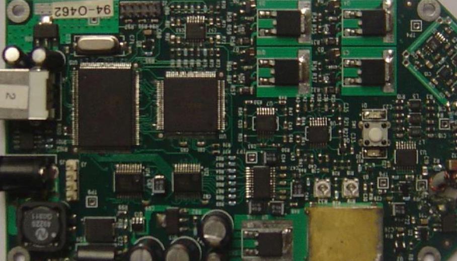
PCB jigsaw technology and PCB test hole design
The size of printed circuit boardof single room shall be determined according to the overall structure of the whole machine The size and shape of the printed circuit board shall be suitable for the surface assembly production line production, conform to the size range of the substrate applICable to the printing machine and the mounter, and the working width of the reflow soldering furnace
Due to the SMAll scale of small and medium-sized enterprises, in order to be more suitable for SMT automatic production, multiple circuit boards are usually combined into one circuit board, and several PCBs of the same unit are consciously combined into rectangles or squares, which is calLED jigsaw puzzle boards
The use of splice plates for small PCBs can improve production efficiency, improve the applicability of production lines, and reduce mold preparation costs. The single side of the printed circuit board is installed on the same side, and the double side full installation without wave soldering can use the double side number front and back of the board. The graphics on both sides are arranged in the same way. This arrangement can improve the utilization rate of equipment (under the condition of medium and small batch production, each investment can be reduced by half), and save production preparation costs and time.
Workpieces can be combined through V-groove linear division, punching, punching and other technological means, which require accurate carving, uniform depth, good mechanical support strength, but are easy to be broken by the divider or by hand.
It is also possible to assemble printed circuit boards with small but identical printed circuits according to this principle, but attention should be paid to the method of compiling component tag numbers.
(1) The drawing board can be composed of multiple identical PCBs or multiple different PCBs.
(2) Determine the maximum size of the stamp plate according to the conditions of the surface assembly equipment, such as the placement area of the mounting machine, the maximum printing area of the printing machine and the working width of the reflux conveyor belt.
design of PCB Test Points and Test Holes
In order to ensure the quality of SMT batch production and reduce costs, online testing is essential The design of the test points and test holes (electrical connection holes used for the electrical performance testing of PCB and PCB components) should be considered during PCB design
(1) Contact reliability test design. In principle, the test points should be located on the same surface and evenly distributed. The diameter of the gasket at the test point is 09mm~1.0mm, and it is matched with the relevant test pin. The center of the test point shall be placed on the grid. Be careful not to design it within 5mm of the plate edge. The center distance between adjacent test points shall not be less than 1.46mm.
PCB Test Point and Test Hole Design Contact Reliability Test Design
Other components shall not be designed between test points, and the distance between test points and component pads shall not be less than 1mm to prevent short circuit between components or test points. It shall be noted that test points shall not be coated with any insulating layer.
Design of PCBTest Points and Test Holes
In principle, the test hole can be replaced by the process hole, but when testing the single board of the panel, the test hole should still be designed on the sub board.
(2) In the power reliability test design, all power nodes shall be provided with test points, that is, the test points shall be able to cover all I/O, power grounding and return signals, and each IC shall have power and grounding test points. If the equipment has multiple power and ground pins, add test points separately. The power supply and grounding of the integrated block shall be placed within 2.54mm, and the IC control wire cannot be directly connected to the power supply, grounding or common resistance. VLSI and ASIC devices with boundary scan devices shall be added as auxiliary test points to realize boundary scan functions, such as clock, mode, data serial input/output terminals, reset terminals, to test the internal functional logic of the device itself.
The size of printed circuit boardof single room shall be determined according to the overall structure of the whole machine The size and shape of the printed circuit board shall be suitable for the surface assembly production line production, conform to the size range of the substrate applICable to the printing machine and the mounter, and the working width of the reflow soldering furnace
Due to the SMAll scale of small and medium-sized enterprises, in order to be more suitable for SMT automatic production, multiple circuit boards are usually combined into one circuit board, and several PCBs of the same unit are consciously combined into rectangles or squares, which is calLED jigsaw puzzle boards
The use of splice plates for small PCBs can improve production efficiency, improve the applicability of production lines, and reduce mold preparation costs. The single side of the printed circuit board is installed on the same side, and the double side full installation without wave soldering can use the double side number front and back of the board. The graphics on both sides are arranged in the same way. This arrangement can improve the utilization rate of equipment (under the condition of medium and small batch production, each investment can be reduced by half), and save production preparation costs and time.
Workpieces can be combined through V-groove linear division, punching, punching and other technological means, which require accurate carving, uniform depth, good mechanical support strength, but are easy to be broken by the divider or by hand.
It is also possible to assemble printed circuit boards with small but identical printed circuits according to this principle, but attention should be paid to the method of compiling component tag numbers.
(1) The drawing board can be composed of multiple identical PCBs or multiple different PCBs.
(2) Determine the maximum size of the stamp plate according to the conditions of the surface assembly equipment, such as the placement area of the mounting machine, the maximum printing area of the printing machine and the working width of the reflux conveyor belt.

design of PCB Test Points and Test Holes
In order to ensure the quality of SMT batch production and reduce costs, online testing is essential The design of the test points and test holes (electrical connection holes used for the electrical performance testing of PCB and PCB components) should be considered during PCB design
(1) Contact reliability test design. In principle, the test points should be located on the same surface and evenly distributed. The diameter of the gasket at the test point is 09mm~1.0mm, and it is matched with the relevant test pin. The center of the test point shall be placed on the grid. Be careful not to design it within 5mm of the plate edge. The center distance between adjacent test points shall not be less than 1.46mm.
PCB Test Point and Test Hole Design Contact Reliability Test Design
Other components shall not be designed between test points, and the distance between test points and component pads shall not be less than 1mm to prevent short circuit between components or test points. It shall be noted that test points shall not be coated with any insulating layer.
Design of PCBTest Points and Test Holes
In principle, the test hole can be replaced by the process hole, but when testing the single board of the panel, the test hole should still be designed on the sub board.
(2) In the power reliability test design, all power nodes shall be provided with test points, that is, the test points shall be able to cover all I/O, power grounding and return signals, and each IC shall have power and grounding test points. If the equipment has multiple power and ground pins, add test points separately. The power supply and grounding of the integrated block shall be placed within 2.54mm, and the IC control wire cannot be directly connected to the power supply, grounding or common resistance. VLSI and ASIC devices with boundary scan devices shall be added as auxiliary test points to realize boundary scan functions, such as clock, mode, data serial input/output terminals, reset terminals, to test the internal functional logic of the device itself.
Application of SMT chip in LED
12-04,2022


抖音二維碼

Q Q二維碼

微信二維碼
點擊
然后
聯(lián)系
然后
聯(lián)系
電話熱線
13410863085Q Q

微信

- 郵箱